


 Dan’s Biz Bookshelf: Four Important Books You Need to Read (Not Just Say You Have)
 The Marketing Minute: Cracking the Code of Technical Marketing


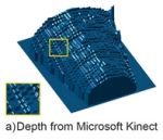
MIT researchers have shown that by exploiting the polarization of light — the physical phenomenon behind polarized sunglasses and most 3-D movie systems — they can increase the resolution of conventional 3-D imaging devices as much as 1,000 times.
The technique could lead to high-quality 3-D cameras built into cellphones, and perhaps to the ability to snap a photo of an object and then use a 3-D printer to produce a replica.
Further out, the work could also abet the development of driverless cars.
“Today, they can miniaturize 3-D cameras to fit on cellphones,” says Achuta Kadambi, a PhD student in the MIT Media Lab and one of the system’s developers. “But they make compromises to the 3-D sensing, leading to very coarse recovery of geometry. That’s a natural application for polarization, because you can still use a low-quality sensor, and adding a polarizing filter gives you something that’s better than many machine-shop laser scanners.”
The researchers describe the new system, which they call Polarized 3D, in a paper they’re presenting at the International Conference on Computer Vision in December. Kadambi is the first author, and he’s joined by his thesis advisor, Ramesh Raskar, associate professor of media arts and sciences in the MIT Media Lab; Boxin Shi, who was a postdoc in Raskar’s group and is now a research fellow at the Rapid-Rich Object Search Lab; and Vage Taamazyan, a master’s student at the Skolkovo Institute of Science and Technology in Russia, which MIT helped found in 2011.
Page 1 of 3
Share on:


Testimonial
"Advertising in PCB007 Magazine has been a great way to showcase our bare board testers to the right audience. The I-Connect007 team makes the process smooth and professional. We’re proud to be featured in such a trusted publication."
Klaus Koziol - atgSuggested Items
Driving Innovation: Depth Routing Processes—Achieving Unparalleled Precision in Complex PCBs
09/08/2025 | Kurt Palmer -- Column: Driving InnovationIn PCB manufacturing, the demand for increasingly complex and miniaturized designs continually pushes the boundaries of traditional fabrication methods, including depth routing. Success in these applications demands not only on robust machinery but also sophisticated control functions. PCB manufacturers rely on advanced machine features and process methodologies to meet their precise depth routing goals. Here, I’ll explore some crucial functions that empower manufacturers to master complex depth routing challenges.
Polar Instruments Announces Additive Transmission Line Support for Si9000e
08/20/2025 | Polar InstrumentsTransmission lines embedded into the PCB surface are a feature of UHDI constructions. The 2025 fall release of Polar's Si9000e PCB impedance & insertion loss transmission line field solver incorporates eight new single ended, differential and coplanar transmission line structures.
Henniker Plasma Launches Stratus Turnkey Plasma Manufacturing Cell
08/13/2025 | Henniker PlasmaHenniker Plasma, a leading manufacturer of plasma treatment systems, proudly announces the launch of its Stratus Plasma Manufacturing Cell range — a fully integrated, turnkey solution that combines advanced atmospheric plasma surface treatment with robotic automation.
Trouble in Your Tank: Metallizing Flexible Circuit Materials—Mitigating Deposit Stress
08/04/2025 | Michael Carano -- Column: Trouble in Your TankMetallizing materials, such as polyimide used for flexible circuitry and high-reliability multilayer printed wiring boards, provide a significant challenge for process engineers. Conventional electroless copper systems often require pre-treatments with hazardous chemicals or have a small process window to achieve uniform coverage without blistering. It all boils down to enhancing the adhesion of the thin film of electroless copper to these smooth surfaces.
Designers Notebook: Basic PCB Planning Criteria—Establishing Design Constraints
07/22/2025 | Vern Solberg -- Column: Designer's NotebookPrinted circuit board development flows more smoothly when all critical issues are predefined and understood from the start. As a basic planning strategy, the designer must first consider the product performance criteria, then determine the specific industry standards or specifications that the product must meet. Planning also includes a review of all significant issues that may affect the product’s manufacture, performance, reliability, overall quality, and safety.