


 Dan’s Biz Bookshelf: Four Important Books You Need to Read (Not Just Say You Have)
 The Marketing Minute: Cracking the Code of Technical Marketing


New Approaches for Hybrid Solar Cells
December 8, 2015 | Technical University of MunichEstimated reading time: 3 minutes
Using a new procedure researchers at the Technical University of Munich (TUM) and the Ludwig Maximillians University of Munich (LMU) can now produce extremely thin and robust, yet highly porous semiconductor layers. A very promising material – for small, light-weight, flexible solar cells, for example, or electrodes improving the performance of rechargeable batteries.
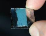
The coating on the wafer that Professor Thomas Fässler, chair of Inorganic Chemistry with a Focus on Novel Materials at TU Munich, holds in his hands glitters like an opal. And it has amazing properties: It is hard as a crystal, exceptionally thin and – since it is highly porous – light as a feather.
By integrating suitable organic polymers into the pores of the material, the scientists can custom tailor the electrical properties of the ensuing hybrid material. The design not only saves space, it also creates large interface surfaces that improve overall effectiveness.
“You can imagine our raw material as a porous scaffold with a structure akin to a honeycomb. The walls comprise inorganic, semiconducting germanium, which can produce and store electric charges. Since the honeycomb walls are extremely thin, charges can flow along short paths,” explains Fässler.
The new design: bottom-up instead of top-down
But, to transform brittle, hard germanium into a flexible and porous layer the researchers had to apply a few tricks. Traditionally, etching processes are used to structure the surface of germanium. However, this top-down approach is difficult to control on an atomic level. The new procedure solves this problem.
Together with his team, Fässler established a synthesis methodology to fabricate the desired structures very precisely and reproducibly. The raw material is germanium with atoms arranged in clusters of nine. Since these clusters are electrically charged, they repel each other as long as they are dissolved. Netting only takes place when the solvent is evaporated.
This can be easily achieved by applying heat of 500 °C or it can be chemically induced, by adding germanium chloride, for example. By using other chlorides like phosphorous chloride the germanium structures can be easily doped. This allows the researchers to directly adjust the properties of the resulting nanomaterials in a very targeted manner.
Page 1 of 2
Share on:


Testimonial
"Our marketing partnership with I-Connect007 is already delivering. Just a day after our press release went live, we received a direct inquiry about our updated products!"
Rachael Temple - AlltematedSuggested Items
Curing and Verification in PCB Shadow Areas
09/17/2025 | Doug Katze, DymaxDesign engineers know a simple truth that often complicates electronics manufacturing: Light doesn’t go around corners. In densely populated PCBs, adhesives and coatings often fail to fully cure in shadowed regions created by tall ICs, connectors, relays, and tight housings.
Marcy’s Musings: Advancing the Advanced Materials Discussion
09/17/2025 | Marcy LaRont -- Column: Marcy's MusingsAs the industry’s most trusted global source of original content about the electronics supply chain, we continually ask you about your concerns, what you care about, and what you most want to learn about. Your responses are insightful and valuable. Thank you for caring enough to provide useful feedback and engage in dialogue.
September 2025 PCB007 Magazine: The Future of Advanced Materials
09/16/2025 | I-Connect007 Editorial TeamMoore’s Law is no more, and the advanced material solutions being developed to grapple with this reality are surprising, stunning, and perhaps a bit daunting. Buckle up for a dive into advanced materials and a glimpse into the next chapters of electronics manufacturing.
I-Connect007 Launches Advanced Electronics Packaging Digest
09/15/2025 | I-Connect007I-Connect007 is pleased to announce the launch of Advanced Electronics Packaging Digest (AEPD), a new monthly digital newsletter dedicated to one of the most critical and rapidly evolving areas of electronics manufacturing: advanced packaging at the interconnect level.
Panasonic Industry will Double the Production Capacity of MEGTRON Multi-layer Circuit Board Materials Over the Next Five Years
09/15/2025 | Panasonic Industry Co., Ltd.Panasonic Industry Co., Ltd., a Panasonic Group company, announced plans for a major expansion of its global production capacity for MEGTRON multi-layer circuit board materials today. The company plans to double its production over the next five years to meet growing demand in the AI server and ICT infrastructure markets.