


 Dan’s Biz Bookshelf: Four Important Books You Need to Read (Not Just Say You Have)
 The Marketing Minute: Cracking the Code of Technical Marketing


Diagnosing Better Efficiencies for Solar Cells
December 14, 2015 | University of MarylandEstimated reading time: 2 minutes
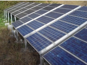
A new diagnostic imaging technique developed by a University of Maryland -led team of researchers promises to boost efficiencies of solar cells by making it possible to find and correct previously undetected ways that solar cells fall far short of theoretical efficiencies.
Theory indicates that current solar cell technologies should able to convert solar energy to electrical energy with at least 30 percent efficiency, but the actual efficiencies of current cells is only around 20 percent. Thus solar panels produce one third less power than the theoretical maximum of these devices.
“With the new imaging technique our team has developed, academic and industry researchers will be able to diagnose where solar cells lose efficiency and close the gap between theory and the actual efficiencies experienced by consumers who install solar panels on their homes and businesses,” said University of Maryland (UMD) Assistant Professor Marina Leite, in the UMD Institute for Research in Electronics and Applied Physics (IREAP) and the department of materials science & engineering in the
A. James Clark School of Engineering.
Solar cell efficiencies depend on the maximum achievable open-circuit voltage generated by the device under illumination. Open-circuit voltage determines how well any photovoltaic device operates, and researchers must be able to measure and image it in order to diagnose which processes are adding to or subtracting from cell efficiency.
The new, ambient temperature imaging technique presented by Leite and her team [Tennyson, et al] is a variation of illuminated Kelvin Probe Force Microscopy, which is a non-contact, non-destructive imaging technique used to determine the composition and electronic state of a surface. Traditionally, this technique uses a laser diode to scan the surface of a solid and measure the potential difference between the tip of the probe and the surface of that material. Tennyson, et al. takes this conventional imaging method further to demonstrate a “direct correlation between Kelvin Probe Force Microscopy measurements (light- minus dark-KPFM) and the open-circuit voltage of photovoltaic devices through the measurement of the quasi-Fermi level splitting”. This indirect measurement allows the UMD-led team to observe precisely [at nanoscale resolution] where the open-circuit voltage is changing.
The researchers say that previous imaging techniques for determining solar cell efficiencies had to be performed under vacuum at very cold temperatures (-333 Fahrenheit or 70 Kelvin). Their new technique fills an important gap in the literature surrounding solar cell efficiencies, providing a “straightforward, universal, and accurate method to measure the open-circuit voltage... with high spatial resolution,” they say.
The findings of Leite and her team are published in, and featured on the cover of, the December 9 issue of Advanced Energy Materials. “Nano-imaging of open-circuit voltage in photovoltaic devices,” Elizabeth Tennyson and Marina Leite*, IREAP and department of materials science & engineering, UMD; Joseph Garrett, IREAP and department of physics, UMD ; Jesse Frantz, Jason Myers, and Jasbinder S. Sanghera, U. S. Naval Research Laboratory; Robel Bekele, University Research Foundation; and Jeremy Munday, department of electrical and computer engineering and IREAP, UMD.
Share on:


Testimonial
"In a year when every marketing dollar mattered, I chose to keep I-Connect007 in our 2025 plan. Their commitment to high-quality, insightful content aligns with Koh Young’s values and helps readers navigate a changing industry. "
Brent Fischthal - Koh YoungSuggested Items
Technica USA Advocates for PCBAA Membership Among Printed Circuit Assembly Customers
09/16/2025 | Technica USATechnica USA is actively encouraging its printed circuit assembly customers to join the Printed Circuit Board Association of America (PCBAA), a leading industry organization advocating for increased domestic production of printed circuit boards (PCBs) and substrates.
American Standard Circuits to Exhibit and Host Lunch & Learn at PCB West 2025
09/17/2025 | American Standard CircuitsAnaya Vardya, President, and CEO of American Standard Circuits/ASC Sunstone Circuits has announced that his company will once again be exhibiting at PCB West 2025 to be held at the Santa Clara Convention Center on Wednesday, October 1, 2025.
Panasonic Industry will Double the Production Capacity of MEGTRON Multi-layer Circuit Board Materials Over the Next Five Years
09/15/2025 | Panasonic Industry Co., Ltd.Panasonic Industry Co., Ltd., a Panasonic Group company, announced plans for a major expansion of its global production capacity for MEGTRON multi-layer circuit board materials today. The company plans to double its production over the next five years to meet growing demand in the AI server and ICT infrastructure markets.
Zhen Ding Expands PCB into Semiconductors at SEMICON Taiwan 2025; Advantech Drives AI Smart Parks
09/12/2025 | Zhen DingZhen Ding Technology Holding Co., Ltd., a global leader in the PCB industry, returned to exhibit at SEMICON Taiwan 2025. Positioning itself as an industry pioneer in "PCB expanding into semiconductors," the company showcased its latest strategic layout
Zhen Ding Technology Highlights AI-Driven Transformation of the PCB Industry at SEMICON Taiwan 2025
09/11/2025 | Zhen Ding TechnologyArtificial intelligence (AI) is expanding rapidly, with almost no field left untouched by the wave of computing power-driven transformation.