


 Dan’s Biz Bookshelf: Four Important Books You Need to Read (Not Just Say You Have)
 The Marketing Minute: Cracking the Code of Technical Marketing


Building Blocks for GaN Power Switches
December 28, 2015 | AIP.orgEstimated reading time: 4 minutes
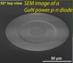
A team of engineers from Cornell University, the University of Notre Dame and the semiconductor company IQE has created gallium nitride (GaN) power diodes capable of serving as the building blocks for future GaN power switches — with applications spanning nearly all electronics products and electricity distribution infrastructures.
Power semiconductor devices are a critical part of the energy infrastructure — all electronics rely on them to control or convert electrical energy. Silicon-based semiconductors are rapidly approaching their performance limits within electronics, so materials such as GaN are being explored as potential replacements that may render silicon switches obsolete.
But along with having many desirable features as a material, GaN is notorious for its defects and reliability issues. So the team zeroed in on devices based on GaN with record-low defect concentrations to probe GaN’s ultimate performance limits for power electronics. They describe their results in a paper in the journal Applied Physics Letters, from AIP Publishing.
“Our engineering goal is to develop inexpensive, reliable, high-efficiency switches to condition electricity — from where it’s generated to where it’s consumed within electric power systems — to replace generations-old, bulky, and inefficient technologies,” said Zongyang Hu, a postdoc working in Professor Grace Huili Xing’s research group within the School of Electrical and Computer Engineering at Cornell University. “GaN-based power devices are enabling technologies to achieve this goal.”
The team examined semiconductor p-n junctions, made by joining p-type (free holes) and n-type (free electrons) semiconductor materials, which have direct applications in solar cells, light-emitting diodes (LEDs), rectifiers in circuits, and numerous variations in more complex devices such as power transistors. “For our work, high-voltage p-n junction diodes are used to probe the material properties of GaN,” Hu explained.
To describe how much the device’s current-voltage characteristics deviate from the ideal case in a defect-free semiconductor system, the team uses a “diode ideality factor.” This is “an extremely sensitive indicator of the bulk defects, interface and surface defects, and resistance of the device,” he added.
Defects exist within all materials, but at varying levels. “So one parameter we used to effectively describe the defect level in a material is the Shockley-Read-Hall (SRH) recombination lifetime,” Hu said.
Page 1 of 2
Share on:


Testimonial
"The I-Connect007 team is outstanding—kind, responsive, and a true marketing partner. Their design team created fresh, eye-catching ads, and their editorial support polished our content to let our brand shine. Thank you all! "
Sweeney Ng - CEE PCBSuggested Items
Electrodeposited Copper Foils Market to Grow by $11.7 Billion Over 2025-2032
09/18/2025 | Globe NewswireThe global electrodeposited copper foils market is poised for dynamic growth, driven by the rising adoption in advanced electronics and renewable energy storage solutions.
Breakthrough in Non-Contact Solder Removal Earns Kurtz Ersa 2025 Mexico Technology Award at SMTA Guadalajara
09/18/2025 | Kurtz Ersa Inc.Kurtz Ersa Inc., a leading supplier of electronics production equipment, is proud to announce that it has been awarded a 2025 Mexico Technology Award in the category of Rework & Repair for its HR 600P Automatic Rework System.
A.R.T. Invests in Latest Equipment to Further Enhance Electronics Training Facilities
09/17/2025 | A.R.T. Ltd.Advanced Rework Technology Ltd. (A.R.T.), a leading independent IPC-accredited training provider, has announced a series of new equipment investments at its state-of-the-art training centre.
Richardson Electronics Appoints Daniel Albers to Drive Made-in-USA Contract Manufacturing Expansion
09/17/2025 | Globe NewswireRichardson Electronics, Ltd., a global provider of engineered solutions for the green energy, power management, and custom display markets, announced the appointment of Daniel Albers to spearhead business development for its expanded, Made-in-USA contract manufacturing efforts.
STMicroelectronics to Advance Next-generation Chip Manufacturing Technology with New PLP Pilot Line in Tours, France
09/17/2025 | STMicroelectronicsSTMicroelectronics, a global semiconductor leader serving customers across the spectrum of electronics applications, today announced new details regarding the development of the next generations of Panel-Level Packaging (PLP) technology through a pilot line in its Tours site, France, which is expected to be operational in Q3 2026.