


 Dan's Biz Bookshelf: 'Getting Naked: A Business Fable'
 The Chemical Connection: Common Misconceptions in Wet Processing
 It’s Only Common Sense: Selling to Engineers


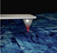
New Acoustic Technique Reveals Structural Information in Nanoscale Materials
December 29, 2015 | Georgia Institute of TechnologyEstimated reading time: 4 minutes
Understanding where and how phase transitions occur is critical to developing new generations of the materials used in high-performance batteries, sensors, energy-harvesting devices, medical diagnostic equipment and other applications. But until now there was no good way to study and simultaneously map these phenomena at the relevant length scales.
Now, researchers at the Georgia Institute of Technology and Oak Ridge National Laboratory (ORNL) have developed a new nondestructive technique for investigating these material changes by examining the acoustic response at the nanoscale. Information obtained from this technique - which uses electrically-conductive atomic force microscope (AFM) probes - could guide efforts to design materials with enhanced properties at small size scales.
The approach has been used in ferroelectric materials, but could also have applications in ferroelastics, solid protonic acids and materials known as relaxors. Sponsored by the National Science Foundation and the Department of Energy's Office of Science, the research was reported December 15 in the journal Advanced Functional Materials.
"We have developed a new characterization technique that allows us to study changes in the crystalline structure and changes in materials behavior at substantially smaller length scales with a relatively simple approach," said Nazanin Bassiri-Gharb, an associate professor in Georgia Tech's Woodruff School of Mechanical Engineering. "Knowing where these phase transitions happen and at which length scales can help us design next-generation materials."
In ferroelectric materials such as PZT (lead zirconate titanate), phase transitions can occur at the boundaries between one crystal type and another, under external stimuli. Properties such as the piezoelectric and dielectric effects can be amplified at the boundaries, which are caused by the multi-element "confused chemistry" of the materials. Determining when these transitions occur can be done in bulk materials using various techniques, and at the smallest scales using an electron microscope.
Page 1 of 2
Share on:


Suggested Items
New Database of Materials Accelerates Electronics Innovation
05/02/2025 | ACN NewswireIn a collaboration between Murata Manufacturing Co., Ltd., and the National Institute for Materials Science (NIMS), researchers have built a comprehensive new database of dielectric material properties curated from thousands of scientific papers.
DuPont Announces Additional Leaders and Company Name for the Intended Spin-Off of the Electronics Business
04/29/2025 | PRNewswireDuPont announced Qnity Electronics, Inc. as the name of the planned independent Electronics public company that will be created through the intended spin-off of its Electronics business.
2024 Global Semiconductor Materials Market Posts $67.5 Billion in Revenue
04/29/2025 | SEMIGlobal semiconductor materials market revenue increased 3.8% to $67.5 billion in 2024, SEMI, the global industry association representing the electronics design and manufacturing supply chain, reported in its Materials Market Data Subscription (MMDS).
New RF Materials Offer Options for RF Designers
04/29/2025 | Andy Shaughnessy, Design007 MagazineThe RF materials arena has changed quite a bit in the past decade. The newest thermoset laminates boast performance numbers that are almost competitive with PTFE, but without the manufacturability challenges. At IPC APEX EXPO this year, I spoke with Brent Mayfield, business development manager at AGC Multi Material America. Brent walked through some recent innovations in RF materials, advances in resin systems, and the many design trade-offs for RF engineers to consider for each material set.
Discovery Opens Doors for Cheaper and Quicker Battery Manufacturing
04/23/2025 | PNNLThe discovery centers on sublimation, a commonly known process whereby under the right conditions, a solid turns directly into a vapor. Sublimation is what creates the tail of a comet as it flies by the sun. As the comet’s icy shell heats up, the ice instantly becomes vapor, instead of first melting into liquid water.