


 The Right Approach: Get Ready for ISO 9001 Version 6
 Dan’s Biz Bookshelf: ‘Still Broke: Walmart’s Remarkable Transformation'
 Driving Innovation: Depth Routing Processes—Achieving Unparalleled Precision in Complex PCBs


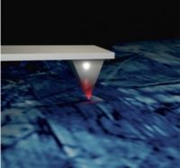
New Acoustic Technique Reveals Structural Information in Nanoscale Materials
December 29, 2015 | Georgia Institute of TechnologyEstimated reading time: 4 minutes
Understanding where and how phase transitions occur is critical to developing new generations of the materials used in high-performance batteries, sensors, energy-harvesting devices, medical diagnostic equipment and other applications. But until now there was no good way to study and simultaneously map these phenomena at the relevant length scales.
Now, researchers at the Georgia Institute of Technology and Oak Ridge National Laboratory (ORNL) have developed a new nondestructive technique for investigating these material changes by examining the acoustic response at the nanoscale. Information obtained from this technique - which uses electrically-conductive atomic force microscope (AFM) probes - could guide efforts to design materials with enhanced properties at small size scales.
The approach has been used in ferroelectric materials, but could also have applications in ferroelastics, solid protonic acids and materials known as relaxors. Sponsored by the National Science Foundation and the Department of Energy's Office of Science, the research was reported December 15 in the journal Advanced Functional Materials.
"We have developed a new characterization technique that allows us to study changes in the crystalline structure and changes in materials behavior at substantially smaller length scales with a relatively simple approach," said Nazanin Bassiri-Gharb, an associate professor in Georgia Tech's Woodruff School of Mechanical Engineering. "Knowing where these phase transitions happen and at which length scales can help us design next-generation materials."
In ferroelectric materials such as PZT (lead zirconate titanate), phase transitions can occur at the boundaries between one crystal type and another, under external stimuli. Properties such as the piezoelectric and dielectric effects can be amplified at the boundaries, which are caused by the multi-element "confused chemistry" of the materials. Determining when these transitions occur can be done in bulk materials using various techniques, and at the smallest scales using an electron microscope.
Page 1 of 2
Share on:


Testimonial
"We’re proud to call I-Connect007 a trusted partner. Their innovative approach and industry insight made our podcast collaboration a success by connecting us with the right audience and delivering real results."
Julia McCaffrey - NCAB GroupSuggested Items
Fresh PCB Concepts: Designing for Success at the Rigid-flex Transition Area
08/28/2025 | Team NCAB -- Column: Fresh PCB ConceptsRigid-flex PCBs come in all shapes and sizes. Manufacturers typically use fire-retardant, grade 4 (FR-4) materials in the rigid section and flexible polyimide materials in the flex region. Because of the small size, some rigid-flex PCBs, like those for hearing aid devices, are among the most challenging to manufacture. However, regardless of its size, we should not neglect the transition area between the rigid and flexible material.
Global Sourcing Spotlight: How to Evaluate Supplier Capabilities Worldwide
08/20/2025 | Bob Duke -- Column: Global Sourcing SpotlightIn global sourcing, the difference between a competitive edge and a catastrophic disruption often comes down to how well you vet your suppliers. Sourcing advanced PCBs, precision components, or materials for complex assemblies demands diligence, skepticism, and more than a little time on airplanes. Here’s how to do your due diligence when evaluating international suppliers and why cutting corners can cost you more than money.
Insulectro and Electroninks Sign North American Distribution Agreement
08/12/2025 | InsulectroElectroninks, a leader in metal organic decomposition (MOD) inks for additive manufacturing and advanced semiconductor packaging, today announced a strategic collaboration and distribution partnership with Insulectro, a premier distributor of materials used in printed electronics and advanced interconnect manufacturing.
Happy’s Tech Talk #41: Sustainability and Circularity for Electronics Manufacturing
08/13/2025 | Happy Holden -- Column: Happy’s Tech TalkI attended INEMI’s June 12 online seminar, “Sustainable Electronics Tech Topic Series: PCBs and Sustainability.” Dr. Maarten Cauwe of imec spoke on “Life Cycle Inventory (LCI) Models for Assessing and Improving the Environmental Impact of PCB Assemblies,” and Jack Herring of Jiva Materials Ltd. spoke on “Transforming Electronics with Recyclable PCB Technology.” This column will review information and provide analysis from both presentations.
Dymax Renews Connecticut Headquarters Lease, Reinforces Long-Term Commitment to Local Community
08/08/2025 | DymaxDymax, a global manufacturer of rapid light-curing materials and equipment, is pleased to announce the renewal and extension of its corporate lease at its 318 Industrial Lane, Torrington, headquarters.