


 Dan’s Biz Bookshelf: Four Important Books You Need to Read (Not Just Say You Have)
 The Marketing Minute: Cracking the Code of Technical Marketing


Simultaneous Detection of the Polarities of Hundreds of Nanowires
January 4, 2016 | Universitat de ValènciaEstimated reading time: 2 minutes
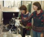
Researchers at the University of Valencia have developed a technique to determine the individual polarities of hundreds of semiconducting nanowires in a single, time-saving process. Led by Ana Cros, director of the University’s Materials Science Institute (ICMUV), the study constitutes a major step forward in both our understanding and application of these structures, since their polarity defines the properties of devices made from them.
Semiconducting nanowires are structures just tens of nanometres in diameter with a typical length-to-width ratio of around 1000 – like a human hair, only a thousand times smaller. So much so that they are often referred to as one-dimensional materials, and indeed they have many interesting properties not seen in larger 3D materials. Semiconducting nanowires are currently among the most-studied nanometric structures and are the basic building blocks for a range of optoelectronic devices that source, detect and control light, such as light detectors, emittors and nanosensors.
Until now, determining their polarities required the nanowires to be analysed one-by-one as part of a complex and time-consuming process. This new technique uses an atomic-strength microscope and a Kelvin probe to detect minuscule forces and measure the electrical characteristics of the sample’s surface. When combined with advanced data analysis, these measurements reveal the polarities of hundreds of nanowires at the same time.
Ana Cros offers us an analogy: “Our microscope explores the surface of the sample in the same way that a blind person explores their surroundings: it uses a probe as a cane, getting an idea as to surface properties based on changes in vibrations. The difference between the microscope and the cane is that its point is extremely sharp. If we then add the electrical charge, we are able to measure the electrical characteristics of the surface of very small objects without even needing to touch them.”
Known as Kelvin probe force microscopy (KPFM), this technique has made it possible to determine the individual polarities of over 100 nanowires at the same time. Núria Garro, researcher at the ICMUV, explains: “What used to take days -having to select the nanowires one-by-one and ultimately destroying the sample- now takes a matter of hours, without incurring any damage whatsoever to the sample”.
The study was published in the journal Nano Letters and was carried out jointly with the University of Murcia, the University of Grenoble and the French Atomic Energy Commission. It constitutes one of the primary findings from a new line of research opened at ICMUV for the study of optoelectronic processes in advanced materials and surfaces. It was carried out as part of the European NANOWIRING project (FP7-People).
Share on:


Testimonial
"In a year when every marketing dollar mattered, I chose to keep I-Connect007 in our 2025 plan. Their commitment to high-quality, insightful content aligns with Koh Young’s values and helps readers navigate a changing industry. "
Brent Fischthal - Koh YoungSuggested Items
Driving Innovation: Depth Routing Processes—Achieving Unparalleled Precision in Complex PCBs
09/08/2025 | Kurt Palmer -- Column: Driving InnovationIn PCB manufacturing, the demand for increasingly complex and miniaturized designs continually pushes the boundaries of traditional fabrication methods, including depth routing. Success in these applications demands not only on robust machinery but also sophisticated control functions. PCB manufacturers rely on advanced machine features and process methodologies to meet their precise depth routing goals. Here, I’ll explore some crucial functions that empower manufacturers to master complex depth routing challenges.
Polar Instruments Announces Additive Transmission Line Support for Si9000e
08/20/2025 | Polar InstrumentsTransmission lines embedded into the PCB surface are a feature of UHDI constructions. The 2025 fall release of Polar's Si9000e PCB impedance & insertion loss transmission line field solver incorporates eight new single ended, differential and coplanar transmission line structures.
Henniker Plasma Launches Stratus Turnkey Plasma Manufacturing Cell
08/13/2025 | Henniker PlasmaHenniker Plasma, a leading manufacturer of plasma treatment systems, proudly announces the launch of its Stratus Plasma Manufacturing Cell range — a fully integrated, turnkey solution that combines advanced atmospheric plasma surface treatment with robotic automation.
Trouble in Your Tank: Metallizing Flexible Circuit Materials—Mitigating Deposit Stress
08/04/2025 | Michael Carano -- Column: Trouble in Your TankMetallizing materials, such as polyimide used for flexible circuitry and high-reliability multilayer printed wiring boards, provide a significant challenge for process engineers. Conventional electroless copper systems often require pre-treatments with hazardous chemicals or have a small process window to achieve uniform coverage without blistering. It all boils down to enhancing the adhesion of the thin film of electroless copper to these smooth surfaces.
Designers Notebook: Basic PCB Planning Criteria—Establishing Design Constraints
07/22/2025 | Vern Solberg -- Column: Designer's NotebookPrinted circuit board development flows more smoothly when all critical issues are predefined and understood from the start. As a basic planning strategy, the designer must first consider the product performance criteria, then determine the specific industry standards or specifications that the product must meet. Planning also includes a review of all significant issues that may affect the product’s manufacture, performance, reliability, overall quality, and safety.