


 Dan’s Biz Bookshelf: Four Important Books You Need to Read (Not Just Say You Have)
 The Marketing Minute: Cracking the Code of Technical Marketing


New Bimetallic Alloy Nanoparticles for Printed Electronic Circuits
January 6, 2016 | TOYOHASHI UNIVERSITY OF TECHNOLOGYEstimated reading time: 1 minute
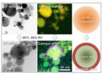
"Printed electronics" has the potential to enable low-cost fabrication of electronics on flexible or curved surfaces, which will lead to the use of electronics in more varied applications. We will be able to fabricate homemade mobile phones or smart watches using a printer in the future. However, the low performance and high cost of current conductive inks limit the advancement of printed electronics.
Now, researchers at Toyohashi Tech and Duke University have found a way to produce new copper alloy nanoparticles, which can be used as the main component of affordable conductive inks with high oxidation resistance. The researchers electrically exploded alloy or twisted metal wires in water with a mild reducing agent (Vitamin C) in order to produce the nanoparticles. The reduction in conductivity was subsequently measured under harsh conditions (high temperature and high humidity).
"We have been working on developing a 'wire explosion' method to produce novel metal nanoparticles. Then, we found that some of the produced copper alloy nanoparticles possessed both high oxidation resistance and low electrical resistance," explains Assistant Professor Go Kawamura. "Moreover, the nanoparticles have the advantage of being inexpensive because the production process is very economical and environmentally friendly."
As a result, copper nanoparticles alloyed with 1% Sn, 5% Ag, 5% Ni, or 30% Ni had electrical conductivities similar to that of copper; however, unlike copper, the nanoparticles remained conductive after 24 h at 85 °C and 85% relative humidity. With further improvement of the electrical conductivity and oxidation resistance, copper alloy nanoparticles prepared by wire explosion could be used for the production of high-performance affordable conductive inks, which will contribute to the advancement of printed electronics. The researchers also hope this work motivates additional study of combining wire explosion with chemical modification of the explosion medium to control the composition and surface chemistry of nanoparticles.
Share on:


Testimonial
"We’re proud to call I-Connect007 a trusted partner. Their innovative approach and industry insight made our podcast collaboration a success by connecting us with the right audience and delivering real results."
Julia McCaffrey - NCAB GroupSuggested Items
Electrodeposited Copper Foils Market to Grow by $11.7 Billion Over 2025-2032
09/18/2025 | Globe NewswireThe global electrodeposited copper foils market is poised for dynamic growth, driven by the rising adoption in advanced electronics and renewable energy storage solutions.
Breakthrough in Non-Contact Solder Removal Earns Kurtz Ersa 2025 Mexico Technology Award at SMTA Guadalajara
09/18/2025 | Kurtz Ersa Inc.Kurtz Ersa Inc., a leading supplier of electronics production equipment, is proud to announce that it has been awarded a 2025 Mexico Technology Award in the category of Rework & Repair for its HR 600P Automatic Rework System.
A.R.T. Invests in Latest Equipment to Further Enhance Electronics Training Facilities
09/17/2025 | A.R.T. Ltd.Advanced Rework Technology Ltd. (A.R.T.), a leading independent IPC-accredited training provider, has announced a series of new equipment investments at its state-of-the-art training centre.
Richardson Electronics Appoints Daniel Albers to Drive Made-in-USA Contract Manufacturing Expansion
09/17/2025 | Globe NewswireRichardson Electronics, Ltd., a global provider of engineered solutions for the green energy, power management, and custom display markets, announced the appointment of Daniel Albers to spearhead business development for its expanded, Made-in-USA contract manufacturing efforts.
STMicroelectronics to Advance Next-generation Chip Manufacturing Technology with New PLP Pilot Line in Tours, France
09/17/2025 | STMicroelectronicsSTMicroelectronics, a global semiconductor leader serving customers across the spectrum of electronics applications, today announced new details regarding the development of the next generations of Panel-Level Packaging (PLP) technology through a pilot line in its Tours site, France, which is expected to be operational in Q3 2026.