


 Dan’s Biz Bookshelf: Four Important Books You Need to Read (Not Just Say You Have)
 The Marketing Minute: Cracking the Code of Technical Marketing


Spooky Interference at a Distance
January 7, 2016 | University of TwenteEstimated reading time: 2 minutes
Nanotechnologists at the University of Twente research institute MESA+ have discovered a new fundamental property of electrical currents in very small metal circuits. They show how electrons can spread out over the circuit like waves and cause interference effects at places where no electrical current is driven. The geometry of the circuit plays a key role in this so called nonlocal effect. The interference is a direct consequence of the quantum mechanical wave character of electrons and the specific geometry of the circuit. For designers of quantum computers it is an effect to take account of. The results are published in the British journal Scientific Reports.
Interference is a common phenomenon in nature and occurs when one or more propagating waves interact coherently. Interference of sound, light or water waves is well known, but also the carriers of electrical current – electrons – can interfere. It shows that electrons need to be considered as waves as well, at least in nanoscale circuits at extremely low temperatures: a canonical example of the quantum mechanical wave-particle duality.
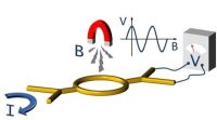
Gold ring
The researchers from the University of Twente have demonstrated electron interference in a gold ring with a diameter of only 500 nanometers (a nanometer is a million times smaller than a millimeter). One side of the ring was connected to a miniature wire through which an electrical current can be driven. On the other side, the ring was connected to a wire with a voltmeter attached to it. When a current was applied, and a varying magnetic field was sent through the ring, the researchers detected electron interference at the other side of the ring, even though no net current flowed through the ring.
This shows that the electron waves can “leak” into the ring, and change the electrical properties elsewhere in the circuit, even when classically one does not expect anything to happen. Although the gold ring is diffusive (meaning that the electron mean free path is much smaller than the ring), the effect was surprisingly pronounced.
Page 1 of 2
Share on:


Testimonial
"In a year when every marketing dollar mattered, I chose to keep I-Connect007 in our 2025 plan. Their commitment to high-quality, insightful content aligns with Koh Young’s values and helps readers navigate a changing industry. "
Brent Fischthal - Koh YoungSuggested Items
Technica USA Advocates for PCBAA Membership Among Printed Circuit Assembly Customers
09/16/2025 | Technica USATechnica USA is actively encouraging its printed circuit assembly customers to join the Printed Circuit Board Association of America (PCBAA), a leading industry organization advocating for increased domestic production of printed circuit boards (PCBs) and substrates.
American Standard Circuits to Exhibit and Host Lunch & Learn at PCB West 2025
09/17/2025 | American Standard CircuitsAnaya Vardya, President, and CEO of American Standard Circuits/ASC Sunstone Circuits has announced that his company will once again be exhibiting at PCB West 2025 to be held at the Santa Clara Convention Center on Wednesday, October 1, 2025.
Panasonic Industry will Double the Production Capacity of MEGTRON Multi-layer Circuit Board Materials Over the Next Five Years
09/15/2025 | Panasonic Industry Co., Ltd.Panasonic Industry Co., Ltd., a Panasonic Group company, announced plans for a major expansion of its global production capacity for MEGTRON multi-layer circuit board materials today. The company plans to double its production over the next five years to meet growing demand in the AI server and ICT infrastructure markets.
Zhen Ding Expands PCB into Semiconductors at SEMICON Taiwan 2025; Advantech Drives AI Smart Parks
09/12/2025 | Zhen DingZhen Ding Technology Holding Co., Ltd., a global leader in the PCB industry, returned to exhibit at SEMICON Taiwan 2025. Positioning itself as an industry pioneer in "PCB expanding into semiconductors," the company showcased its latest strategic layout
Zhen Ding Technology Highlights AI-Driven Transformation of the PCB Industry at SEMICON Taiwan 2025
09/11/2025 | Zhen Ding TechnologyArtificial intelligence (AI) is expanding rapidly, with almost no field left untouched by the wave of computing power-driven transformation.