


 Dan’s Biz Bookshelf: Four Important Books You Need to Read (Not Just Say You Have)
 The Marketing Minute: Cracking the Code of Technical Marketing


Weaving a New Story for COFS and MOFs
January 22, 2016 | DOE/Lawrence Berkeley National LaboratoryEstimated reading time: 3 minutes
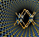
There are many different ways to make nanomaterials but weaving, the oldest and most enduring method of making fabrics, has not been one of them - until now. An international collaboration led by scientists at the U.S. Department of Energy (DOE)'s Lawrence Berkeley National Laboratory (Berkeley Lab) and the University of California (UC) Berkeley, has woven the first three-dimensional covalent organic frameworks (COFs) from helical organic threads. The woven COFs display significant advantages in structural flexibility, resiliency and reversibility over previous COFs - materials that are highly prized for their potential to capture and store carbon dioxide then convert it into valuable chemical products.
"We have taken the art of weaving into the atomic and molecular level, giving us a powerful new way of manipulating matter with incredible precision in order to achieve unique and valuable mechanical properties," says Omar Yaghi, a chemist who holds joint appointments with Berkeley Lab's Materials Sciences Division and UC Berkeley's Chemistry Department, and is the co-director of the Kavli Energy NanoScience Institute (Kavli-ENSI).
"Weaving in chemistry has been long sought after and is unknown in biology," Yaghi says. "However, we have found a way of weaving organic threads that enables us to design and make complex two- and three-dimensional organic extended structures."
Yaghi is the corresponding author of a paper in Science reporting this new technique. The paper is titled "Weaving of organic threads into a crystalline covalent organic framework." The lead authors are Yuzhong Liu, Yanhang Ma and Yingbo Zhao. Other co-authors are Xixi Sun, Felipe Gándara, Hiroyasu Furukawa, Zheng Liu, Hanyu Zhu, Chenhui Zhu, Kazutomo Suenaga, Peter Oleynikov, Ahmad Alshammari, Xiang Zhang and Osamu Terasaki.
Page 1 of 2
Share on:


Testimonial
"Our marketing partnership with I-Connect007 is already delivering. Just a day after our press release went live, we received a direct inquiry about our updated products!"
Rachael Temple - AlltematedSuggested Items
Electrodeposited Copper Foils Market to Grow by $11.7 Billion Over 2025-2032
09/18/2025 | Globe NewswireThe global electrodeposited copper foils market is poised for dynamic growth, driven by the rising adoption in advanced electronics and renewable energy storage solutions.
MacDermid Alpha Showcases Advanced Interconnect Solutions at PCIM Asia 2025
09/18/2025 | MacDermid Alpha Electronics SolutionsMacDermid Alpha Electronic Solutions, a global leader in materials for power electronics and semiconductor assembly, will showcase its latest interconnect innovations in electronic interconnect materials at PCIM Asia 2025, held from September 24 to 26 at the Shanghai New International Expo Centre, Booth N5-E30
Trouble in Your Tank: Implementing Direct Metallization in Advanced Substrate Packaging
09/15/2025 | Michael Carano -- Column: Trouble in Your TankDirect metallization systems based on conductive graphite are gaining popularity throughout the world. The environmental and productivity gains achievable with this process are outstanding. Direct metallization reduces the costs of compliance, waste treatment, and legal issues related to chemical exposure. A graphite-based direct plate system has been devised to address these needs.
Closing the Loop on PCB Etching Waste
09/09/2025 | Shawn Stone, IECAs the PCB industry continues its push toward greener, more cost-efficient operations, Sigma Engineering’s Mecer System offers a comprehensive solution to two of the industry’s most persistent pain points: etchant consumption and rinse water waste. Designed as a modular, fully automated platform, the Mecer System regenerates spent copper etchants—both alkaline and acidic—and simultaneously recycles rinse water, transforming a traditionally linear chemical process into a closed-loop system.
Driving Innovation: Depth Routing Processes—Achieving Unparalleled Precision in Complex PCBs
09/08/2025 | Kurt Palmer -- Column: Driving InnovationIn PCB manufacturing, the demand for increasingly complex and miniaturized designs continually pushes the boundaries of traditional fabrication methods, including depth routing. Success in these applications demands not only on robust machinery but also sophisticated control functions. PCB manufacturers rely on advanced machine features and process methodologies to meet their precise depth routing goals. Here, I’ll explore some crucial functions that empower manufacturers to master complex depth routing challenges.