


 Dan’s Biz Bookshelf: Four Important Books You Need to Read (Not Just Say You Have)
 The Marketing Minute: Cracking the Code of Technical Marketing


Microwaved Nanotubes Come Up Clean
January 25, 2016 | Rice UniversityEstimated reading time: 2 minutes
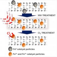
A standard kitchen microwave proved effective as part of a two-step process invented at Rice and Swansea universities to clean carbon nanotubes.
Basic nanotubes are good for many things, like forming into microelectronic components or electrically conductive fibers and composites; for more sensitive uses like drug delivery and solar panels, they need to be as pristine as possible.
Nanotubes form from metal catalysts in the presence of heated gas, but residues of those catalysts (usually iron) sometimes remain stuck on and inside the tubes. The catalyst remnants can be difficult to remove by physical or chemical means because the same carbon-laden gas used to make the tubes lets carbon atoms form encapsulating layers around the remaining iron, reducing the ability to remove it during purification.
In the new process, treating the tubes in open air in a microwave burns off the amorphous carbon. The nanotubes can then be treated with high-temperature chlorine to eliminate almost all of the extraneous particles.
The process was revealed in the Royal Society of Chemistry journal RSC Advances.
The labs of chemists Robert Hauge, Andrew Barron and Charles Dunnill led the study. Barron is a professor at Rice in Houston and at Swansea University in the United Kingdom. Rice’s Hauge is a pioneer in nanotube growth techniques. Dunnill is a senior lecturer at the Energy Safety Research Institute at Swansea.
There are many ways to purify nanotubes, but at a cost, Barron said. “The chlorine method developed by Hauge has the advantage of not damaging the nanotubes, unlike other methods,” he said. “Unfortunately, many of the residual catalyst particles are surrounded by a carbon layer that stops the chlorine from reacting, and this is a problem for making high-purity carbon nanotubes.”
Page 1 of 2
Share on:


Testimonial
"The I-Connect007 team is outstanding—kind, responsive, and a true marketing partner. Their design team created fresh, eye-catching ads, and their editorial support polished our content to let our brand shine. Thank you all! "
Sweeney Ng - CEE PCBSuggested Items
Alternative Manufacturing, Inc. (AMI) Announces Commitment to Excellence in Industrial, Defense, Aerospace, Renewables, and Robotics Markets
09/16/2025 | Alternative Manufacturing, Inc.Alternative Manufacturing, Inc. (AMI), a 100% employee-owned contract manufacturer, proudly reaffirms its leadership in the electronics manufacturing services (EMS) industry with a continued commitment to delivering high-quality PCBAs and box builds across the industrial, defense, aerospace, renewable energy, and robotics markets.
Sustainability and Selective Soldering
09/15/2025 | Dr. Samuel J. McMaster, Pillarhouse InternationalSustainability is more than just a buzzword for the electronics industry; it’s a key goal for all manufacturing processes. This is more than a box-ticking exercise or simply doing a small part for environmentally friendly processes. Moving toward sustainable solutions drives innovation and operational efficiency.
Trouble in Your Tank: Implementing Direct Metallization in Advanced Substrate Packaging
09/15/2025 | Michael Carano -- Column: Trouble in Your TankDirect metallization systems based on conductive graphite are gaining popularity throughout the world. The environmental and productivity gains achievable with this process are outstanding. Direct metallization reduces the costs of compliance, waste treatment, and legal issues related to chemical exposure. A graphite-based direct plate system has been devised to address these needs.
EV Group Achieves Breakthrough in Hybrid Bonding Overlay Control for Chiplet Integration
09/12/2025 | EV GroupEV Group (EVG), a leading provider of innovative process solutions and expertise serving leading-edge and future semiconductor designs and chip integration schemes, today unveiled the EVG®40 D2W—the first dedicated die-to-wafer overlay metrology platform to deliver 100 percent die overlay measurement on 300-mm wafers at high precision and speeds needed for production environments. With up to 15X higher throughput than EVG’s industry benchmark EVG®40 NT2 system designed for hybrid wafer bonding metrology, the new EVG40 D2W enables chipmakers to verify die placement accuracy and take rapid corrective action, improving process control and yield in high-volume manufacturing (HVM).
Integrating Uniplate PLBCu6 With the Digital Factory Suite
09/12/2025 | Giovanni Obino and Andreas Schatz, MKS' AtotechPrinted circuit board manufacturing is rapidly changing, driven by miniaturization, stringent reliability requirements, and growing pressure for sustainable production. Meeting these challenges requires more than incremental improvements; it demands a combination of precise equipment and real-time process intelligence. The pairing of Uniplate® PLBCu6 with the Digital Factory Suite (DFS) demonstrates how hardware and software can work together to create more responsive, resource-efficient manufacturing.