


 Dan’s Biz Bookshelf: Four Important Books You Need to Read (Not Just Say You Have)
 The Marketing Minute: Cracking the Code of Technical Marketing


Petawatt Laser System Passes a Key Milestone
January 25, 2016 | Lawrence Livermore National LaboratoryEstimated reading time: 3 minutes
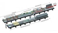
The High-Repetition-Rate Advanced Petawatt Laser System (HAPLS) under construction at LLNL recently achieved a key average power milestone more than two months ahead of schedule, and is now moving into the next phase in its development.
The HAPLS high-energy diode-pumped solid-state pump laser, firing at a repetition rate of 3.3 Hz (3.3 shots per second), achieved 70 joules of infrared (1,053-nanometer) energy and 39 joules of green (527-nm) energy. Completion of this average-power milestone marks another major step in the HAPLS commissioning plan: the beginning of the integration of the pump laser with the HAPLS high-energy short-pulse beamline.
“Ramping the pump laser to this intermediary performance level was an important step for HAPLS,” said Constantin Haefner, program director for Advanced Photon Technologies. “For the first time we ran the pump laser at significant energy and average power levels, meeting and exceeding the required goals for this milestone. This accomplishment required a huge team effort and the team worked extremely hard to make this happen.
“We are taking a risk-balanced approach in ramping HAPLS to its full performance. The data we collected confirmed our performance models and gave the green light to start integration with the short-pulse beamline before ramping to even higher power levels.”
Representatives from the European Union’s Extreme Light Infrastructure Beamlines (link is external) (ELI-Beamlines) facility in the Czech Republic, where HAPLS will be installed, attended the demonstration. “We are delighted to see the HAPLS pump laser work with a performance exceeding the project expectations for this phase, and achieve this important milestone on budget and ahead of schedule,” said ELI Beamlines Chief Laser Scientist Bedrich Rus. “The partnership with LLNL has been a tremendously successful story, and this demonstration shows the robustness of the underlying design and technology. The L3 (HAPLS) beamline will be an ELI Beamlines’ user facility workhorse.”
Page 1 of 2
Share on:


Testimonial
"Advertising in PCB007 Magazine has been a great way to showcase our bare board testers to the right audience. The I-Connect007 team makes the process smooth and professional. We’re proud to be featured in such a trusted publication."
Klaus Koziol - atgSuggested Items
MEMS & Imaging Sensors Summit to Spotlight Sensing Revolution for Europe’s Leadership
09/11/2025 | SEMIIndustry experts will gather November 19-20 at the SEMI MEMS & Imaging Sensors Summit 2025 to explore the latest breakthroughs in AI-driven MEMS and imaging optimization, AR/VR technologies, and advanced sensor solutions for critical defence applications.
Direct Imaging System Market Size to Hit $4.30B by 2032, Driven by Increasing Demand for High-Precision PCB Manufacturing
09/11/2025 | Globe NewswireAccording to the SNS Insider, “The Direct Imaging System Market size was valued at $2.21 Billion in 2024 and is projected to reach $4.30 Billion by 2032, growing at a CAGR of 8.68% during 2025-2032.”
I-Connect007’s Editor’s Choice: Five Must-Reads for the Week
07/04/2025 | Marcy LaRont, I-Connect007For our industry, we have seen several bullish market announcements over the past few weeks, including one this week by IDC on the massive growth in the global server market. We’re also closely watching global trade and nearshoring. One good example of successful nearshoring is Rehm Thermal Systems, which celebrates its 10th anniversary in Mexico and the official opening of its new building in Guadalajara.
Driving Innovation: Direct Imaging vs. Conventional Exposure
07/01/2025 | Simon Khesin -- Column: Driving InnovationMy first camera used Kodak film. I even experimented with developing photos in the bathroom, though I usually dropped the film off at a Kodak center and received the prints two weeks later, only to discover that some images were out of focus or poorly framed. Today, every smartphone contains a high-quality camera capable of producing stunning images instantly.
United Electronics Corporation Advances Manufacturing Capabilities with Schmoll MDI-ST Imaging Equipment
06/24/2025 | United Electronics CorporationUnited Electronics Corporation has successfully installed the advanced Schmoll MDI-ST (XL) imaging equipment at their advanced printed circuit board facility. This significant technology investment represents a continued commitment to delivering superior products and maintaining their position as an industry leader in precision PCB manufacturing.