


 Dan’s Biz Bookshelf: Four Important Books You Need to Read (Not Just Say You Have)
 The Marketing Minute: Cracking the Code of Technical Marketing


New Magnetoresistance Effect Occurring in Materials with Strong Spin-Orbit Coupling
January 27, 2016 | Elhuyar FundazioaEstimated reading time: 2 minutes
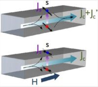
Researchers of the Nanodevices group, in collaboration with groups from the CFM and DIPC, both institutions also located in Donostia-San Sebastián, have discovered a new magnetoresistance effect occurring in materials with strong spin-orbit coupling.
These materials, which include metals such as platinum or tantalum, are characterized for being capable of generating a spin current from an electrical current (and viceversa) by means of the so-called spin Hall effect. For this reason, these materials are of outmost importance in the field of spintronics -the branch of science that is devoted to explore the generation, transmission and detection of spin currents in materials and devices. The ultimate goal of spintronics is to have a deeper understanding of the charge-to-spin conversion and transport phenomena at the nanoscale in order to be able to design new functional and efficient devices that are not only based on the injection, transport and storage of electrical charge, but also to its spin, which could revolutionize the conventional electronics and expand its limits. The researchers show that, by means of this novel magnetoresistive effect, it is now possible to study the spin transport properties in these materials without the need to fabricate complex devices and/or involve interfaces between different materials.
When an electric current is applied to a thin film of a material with strong spin-orbit coupling (typically of a few nanometers thick), a spin current is generated in the transverse direction -that is, along the thickness of the film- via the direct spin Hall effect, which in turn produces an electric current (via the inverse spin Hall effect) that adds to the initial applied current. This effect -small since it is due to a second-order correction-, causes a reduction in the resistivity of the film, and is maximum when the film thickness is on the order of to the spin diffusion length -that is, the average distance that a spin can travel through the material without suffering a collision that may cause a change in its state. If a magnetic field is applied not collinear to the direction where the spins points to, one can force them to precess -via the so-called Hanle effect-, thereby generating a modulation in the resistivity of the material. According to Saul Velez, first author of the work, "this new phenomenon could open ahead the possibility to study the spin transport in materials and systems not yet explored". "This new effect also allows to study the spin transport properties of known materials, and to compare the results with the ones obtained with other techniques or devices", adds Fèlix Casanova, last author and supervisor of the work.
Share on:


Testimonial
"We’re proud to call I-Connect007 a trusted partner. Their innovative approach and industry insight made our podcast collaboration a success by connecting us with the right audience and delivering real results."
Julia McCaffrey - NCAB GroupSuggested Items
Curing and Verification in PCB Shadow Areas
09/17/2025 | Doug Katze, DymaxDesign engineers know a simple truth that often complicates electronics manufacturing: Light doesn’t go around corners. In densely populated PCBs, adhesives and coatings often fail to fully cure in shadowed regions created by tall ICs, connectors, relays, and tight housings.
Marcy’s Musings: Advancing the Advanced Materials Discussion
09/17/2025 | Marcy LaRont -- Column: Marcy's MusingsAs the industry’s most trusted global source of original content about the electronics supply chain, we continually ask you about your concerns, what you care about, and what you most want to learn about. Your responses are insightful and valuable. Thank you for caring enough to provide useful feedback and engage in dialogue.
September 2025 PCB007 Magazine: The Future of Advanced Materials
09/16/2025 | I-Connect007 Editorial TeamMoore’s Law is no more, and the advanced material solutions being developed to grapple with this reality are surprising, stunning, and perhaps a bit daunting. Buckle up for a dive into advanced materials and a glimpse into the next chapters of electronics manufacturing.
I-Connect007 Launches Advanced Electronics Packaging Digest
09/15/2025 | I-Connect007I-Connect007 is pleased to announce the launch of Advanced Electronics Packaging Digest (AEPD), a new monthly digital newsletter dedicated to one of the most critical and rapidly evolving areas of electronics manufacturing: advanced packaging at the interconnect level.
Panasonic Industry will Double the Production Capacity of MEGTRON Multi-layer Circuit Board Materials Over the Next Five Years
09/15/2025 | Panasonic Industry Co., Ltd.Panasonic Industry Co., Ltd., a Panasonic Group company, announced plans for a major expansion of its global production capacity for MEGTRON multi-layer circuit board materials today. The company plans to double its production over the next five years to meet growing demand in the AI server and ICT infrastructure markets.