


 Dan’s Biz Bookshelf: Four Important Books You Need to Read (Not Just Say You Have)
 The Marketing Minute: Cracking the Code of Technical Marketing


The Iron Stepping Stones To Better Wearable Tech Without Semiconductors
February 12, 2016 | Michigan Technological UniversityEstimated reading time: 3 minutes
The road to more versatile wearable technology is dotted with iron. Specifically, quantum dots of iron arranged on boron nitride nanotubes (BNNTs). The new material is the subject of a study published in Scientific Reports in February, led by Yoke Khin Yap, a professor of physics at Michigan Technological University.
Yap says the iron-studded BNNTs are pushing the boundaries of electronics hardware. The transistors modulating electron flow need an upgrade.
“Look beyond semiconductors,” he says, explaining that materials like silicon semiconductors tend to overheat, can only get so small and leak electric current. The key to revamping the fundamental base of transistors is creating a series of stepping-stones.
Quantum Dots
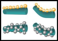
The nanotubes are the mainframe of this new material. BNNTs are great insulators and terrible at conducting electricity. While at first that seems like an odd choice for electronics, the insulating effect of BNNTs is crucial to prevent current leakage and overheating. Additionally, electron flow will only occur across the metal dots on the BNNTs.
In past research, Yap and his team used gold for quantum dots, placed along a BNNT in a tidy line. With enough energy potential, the electrons are repelled by the insulating BNNT and hopscotch from gold dot to gold dot. This electron movement is called quantum tunneling.
“Imagine this as a river, and there’s no bridge; it’s too big to hop over,” Yap says. “Now, picture having stepping stones across the river—you can cross over, but only when you have enough energy to do so.”
Nanotech for Wearable Electronics
Unlike with semiconductors, there is no classical resistance with quantum tunneling. No resistance means no heat. Plus, these materials are very small; the nanomaterials enable the transistors to shrink as well. An added bonus is that BNNTs are also quite flexible, a boon for wearable electronics.
“Here’s where the challenge comes in,” Yap says, holding up a pen to demonstrate. He gestures along the length of the pen, which mimics a straight BNNT, tapping out a line of quantum dots. “We have an array here to do quantum tunneling, but what if we want to bend the array to be flexible like a piece of wearable electronics?”
Yap sets down the pen and curls up his index finger: “And if I bend the dots, the distance between them changes—in doing so, we change the electronic behavior.”
Changing the behavior means that the quantum tunneling may not work. The solution is to get out of line: Yap and his team arranged a grid of quantum dots around the outside of the BNNT.
“This time we used iron instead of gold,” Yap adds, explaining that gold’s melting temperature was low for the process his team used. “And when we tested the material, the electrons distributed uniformly across the whole surface of the nanotubes.”
That means that instead of having a line of stepping stones, there are many different paths across the river, and an electron will jump to the nearest one. For future use in wearable electronics, the multiplicity of paths ensures electricity is moving from one riverbank to the next, one way or another. Using scanning tunneling microscopy inside a transmission electron microscope (STM-TEM), the team successfully bent the iron dot-coated BNNT while monitoring the electron flows. The electronic behaviors remain the same even when the BNNT was bent all the way up to 75 degrees.
Next Steps
Yap says that this experiment is a proof of concept. While the iron BNNT material shows promise, it’s not a full transistor yet, capable of modulating electron movement. Right now, it’s called a flexible tunneling channel.
“Next, we’ll put the BNNT and iron onto a bendable plastic substrate,” Yap says. “Then we’ll bend this substrate and watch where the electrons go.”
This experimental work is complemented by computer simulations by John Jaszczak, professor of physics, and Paul Bergstrom, professor of electrical and computer engineering.
Which route the electricity takes is hard to track, which will be the main challenge for the next experiment. But one direction is certain, Yap’s research is headed down a path to change the basic level of electronics and make wearable tech more adaptable.
Share on:


Testimonial
"Advertising in PCB007 Magazine has been a great way to showcase our bare board testers to the right audience. The I-Connect007 team makes the process smooth and professional. We’re proud to be featured in such a trusted publication."
Klaus Koziol - atgSuggested Items
Curing and Verification in PCB Shadow Areas
09/17/2025 | Doug Katze, DymaxDesign engineers know a simple truth that often complicates electronics manufacturing: Light doesn’t go around corners. In densely populated PCBs, adhesives and coatings often fail to fully cure in shadowed regions created by tall ICs, connectors, relays, and tight housings.
Marcy’s Musings: Advancing the Advanced Materials Discussion
09/17/2025 | Marcy LaRont -- Column: Marcy's MusingsAs the industry’s most trusted global source of original content about the electronics supply chain, we continually ask you about your concerns, what you care about, and what you most want to learn about. Your responses are insightful and valuable. Thank you for caring enough to provide useful feedback and engage in dialogue.
September 2025 PCB007 Magazine: The Future of Advanced Materials
09/16/2025 | I-Connect007 Editorial TeamMoore’s Law is no more, and the advanced material solutions being developed to grapple with this reality are surprising, stunning, and perhaps a bit daunting. Buckle up for a dive into advanced materials and a glimpse into the next chapters of electronics manufacturing.
I-Connect007 Launches Advanced Electronics Packaging Digest
09/15/2025 | I-Connect007I-Connect007 is pleased to announce the launch of Advanced Electronics Packaging Digest (AEPD), a new monthly digital newsletter dedicated to one of the most critical and rapidly evolving areas of electronics manufacturing: advanced packaging at the interconnect level.
Panasonic Industry will Double the Production Capacity of MEGTRON Multi-layer Circuit Board Materials Over the Next Five Years
09/15/2025 | Panasonic Industry Co., Ltd.Panasonic Industry Co., Ltd., a Panasonic Group company, announced plans for a major expansion of its global production capacity for MEGTRON multi-layer circuit board materials today. The company plans to double its production over the next five years to meet growing demand in the AI server and ICT infrastructure markets.