


 Dan’s Biz Bookshelf: Four Important Books You Need to Read (Not Just Say You Have)
 The Marketing Minute: Cracking the Code of Technical Marketing


Ultrathin Semiconductor Heterostructures for New Technological Applications
February 15, 2016 | University of WashingtonEstimated reading time: 4 minutes
Heterostructures formed by different three-dimensional semiconductors form the foundation for modern electronic and photonic devices. Now, University of Washington scientists have successfully combined two different ultrathin semiconductors — each just one layer of atoms thick and roughly 100,000 times thinner than a human hair — to make a new two-dimensional heterostructure with potential uses in clean energy and optically-active electronics. The team, led by Boeing Distinguished Associate Professor Xiaodong Xu, announced its findings in a paper published Feb. 12 in the journal Science.
Senior author Xu and lead authors Kyle Seyler and Pasqual Rivera, both doctoral students in the UW physics department, synthesized and investigated the optical properties of this new type of semiconductor sandwich.
“What we’re seeing here is distinct from heterostructures made of 3-D semiconductors,” said Xu, who has joint appointments in the Department of Physics and the Department of Materials Science and Engineering. “We’ve created a system to study the special properties of these atomically thin layers and their potential to answer basic questions about physics and develop new electronic and photonic technologies.”
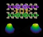
When semiconductors absorb light, pairs of positive and negative charges can form and bind together to create so-called excitons. Scientists have long studied how these excitons behave, but when they are squeezed down to the 2-D limit in these atomically thin materials, surprising interactions can occur.
While traditional semiconductors manipulate the flow of electron charge, this device allows excitons to be preserved in “valleys,” a concept from quantum mechanics similar to the spin of electrons. This is a critical step in the development of new nanoscale technologies that integrate light with electronics.
“It was already known that these ultrathin 2-D semiconductor have these unique properties that you cannot find in other 2-D or 3-D arrangements,” said Xu. “But as we show here, when we put these two layers together — one on top of the other — the interface between these sheets becomes the site of even more new physical properties, which you don’t see in each layer on its own or in the 3-D version.”
Xu and his team wanted to create and explore the properties of a 2-D semiconductor heterostructure made up of two different layers of material, a natural expansion of their previous studies on atomically thin junctions, as well as nanoscale lasers based on atomically thin layers of semiconductors. By studying how laser light interacts with this heterostructure, they gathered information about the physical properties at the atomically sharp interface.
“Many groups have studied the optical properties of single 2-D sheets,” said Seyler. “What we do here is carefully stack one material on top of another, and then study the new properties that arise at the interface.”
The team obtained two types of semiconducting crystals, tungsten diselenide (WSe2) and molybdenum diselenide (MoSe2), from collaborators at Oak Ridge National Laboratory. They used facilities developed in-house to precisely arrange two layers, one derived from each crystal, a process that took a few years to fully develop.
“But now that we know how to do it properly, we can make new ones in one or two weeks,” said Xu.
Getting these devices to emit light posed a unique challenge, due to the properties of electrons in each layer.
“Once you have these two sheets of material, an essential question is how to position the two layers together,” said Seyler. The electrons in each layer have unique spin and valley properties, and “how you position them — their twist angle — affects how they interact with light.”
By aligning the crystal lattices, the authors could excite the heterostructure with a laser and create optically active excitons between the two layers.
“These excitons at the interface can store valley information for orders of magnitude longer than either of the layers on their own,” said Rivera. “This long lifetime allows for fascinating effects which may lead to further optical and electronic applications with valley functionality.”
Now that they can efficiently make a semiconductor heterostructure out of 2-D materials, Xu and his team would like to explore a number of fascinating physical properties, including how exciton behavior varies as they change angles between the layers, the quantum properties excitons between layers and electrically driven light emission.
“There’s a whole industry that wants to use these 2-D semiconductors to make new electronic and photonic devices,” said Xu. “So we’re trying to study the fundamental properties of these new heterostructures for things like efficient laser technology, light-emitting diodes and light-harvesting devices. These will hopefully be useful for clean energy and information technology applications. It is quite exciting but there’s a lot work to do.”
Other co-authors are Hongyi Yu and Wang Yao at the University of Hong Kong; Jiaqiang Yan and David Mandrus at Oak Ridge National Laboratory and the University of Tennessee; and UW physics postdoctoral researcher John Schaibley. The UW authors were primarily funded by the U.S. Department of Energy, with additional support from the UW’s Clean Energy Institute and the National Science Foundation.
Share on:


Testimonial
"Advertising in PCB007 Magazine has been a great way to showcase our bare board testers to the right audience. The I-Connect007 team makes the process smooth and professional. We’re proud to be featured in such a trusted publication."
Klaus Koziol - atgSuggested Items
Kris Moyer Discusses His Emerging Design Technologies Class
09/04/2025 | Marcy LaRont, I-Connect007Kris Moyer, a design instructor for the Global Electronics Association, will be teaching his advanced PCB design class this fall. If you’re ready to level up your design education, you won’t want to miss this interview. The PCB Design for Emerging Design Technologies course is designed to provide the skills necessary to create PCB/PBA designs that require cutting-edge emerging design technologies and comply with all necessary IPC standards, including new standards being developed in this area.
Leadership Change at Koh Young Europe
08/14/2025 | Koh YoungAfter 16 years of leading Koh Young Europe as General Manager, we would like to announce that Harald Eppinger will step down from his executive role.
Driving Innovation: Inner Layer Alignment Methods in PCB Production
08/06/2025 | Kurt Palmer -- Column: Driving InnovationIn PCB manufacturing, precision is a fundamental requirement. Among many complex processes, the accurate registration of inner layers before lamination is one of the most critical. Much like a child's game where rings must be perfectly stacked onto a single pin, PCB manufacturers align multiple conductive and insulating layers to form a cohesive, functional board. This alignment directly affects PCB precision; tighter layer alignment results in smaller "annular rings," superior performance, and higher yields.
From Attraction to Action: Where Marketing Ends and Sales Begins
07/29/2025 | Brittany Martin, I-Connect007Before a PO hits the system, marketing has already done a lot of heavy lifting. Without strategic marketing, the PO might never arrive. At I-Connect007, we have been fortunate to help many companies achieve sales success through marketing. The key to success? Understanding how marketing leads to sales.
Siemens Expands Global Electronics Intelligence Reach and Supplyframe Portfolio with Wevolver Acquisition
04/30/2025 | Siemens Digital Industries SoftwareSiemens Digital Industries Software announced its intention to acquire Wevolver, expanding its audience reach, enhancing the Supplyframe product portfolio, and combining digital marketing and integrated campaign programs that include go-to-market support and content creation.