


 Dan’s Biz Bookshelf: Four Important Books You Need to Read (Not Just Say You Have)
 The Marketing Minute: Cracking the Code of Technical Marketing


Quantum Dot Solids: This Generation's Silicon Wafer?
February 25, 2016 | Cornell UniversityEstimated reading time: 3 minutes
Just as the single-crystal silicon wafer forever changed the nature of electronics 60 years ago, a group of Cornell researchers is hoping its work with quantum dot solids – crystals made out of crystals – can help usher in a new era in electronics.
The multidisciplinary team, led by Tobias Hanrath, associate professor in the Robert Frederick Smith School of Chemical and Biomolecular Engineering, and graduate student Kevin Whitham, has fashioned two-dimensional superstructures out of single-crystal building blocks. Through directed assembly and attachment processes, the lead selenide quantum dots are synthesized into larger crystals, then fused together to form atomically coherent square superlattices.
The difference between these and previous crystalline structures is the atomic coherence of each 5-nanometer crystal (a nanometer is one-billionth of a meter). They’re not connected by a substance between each crystal – they’re connected directly to each other. The electrical properties of these superstructures potentially are superior to existing semiconductor quantum dots, with anticipated applications in solar cells and other electronic devices.
“As far as level of perfection, in terms of making the building blocks and connecting them into these superstructures, that is probably as far as you can push it,” Hanrath said, referring to the atomic-scale precision of the process.
The paper, “Charge transport and localization in atomically coherent quantum dot solids,” is published in the Feb. 22 issue of Nature Materials.
Whitham, a doctoral candidate in the field of materials science and engineering, did most of the experimentation and is lead author of the work. Also contributing were: Jun Yang, postdoctoral researcher; Benjamin H. Savitzky, graduate student in the field of physics; Lena Kourkoutis, assistant professor and Morgan Sesquicentennial Faculty Fellow in applied and engineering physics; and Frank Wise, the Samuel B. Eckert Professor of Engineering.
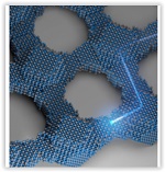
Provided
Associate professor Tobias Hanrath explains his group’s work on assembling quantum dots into ordered, two-dimensional superlattices, the subject of a paper published Feb. 22 in Nature Materials. The work has potential applications in optoelectronics.
This latest work has grown out of previous published research by the Hanrath group, including a 2013 paper published in Nano Letters that reported a new approach to connecting quantum dots through controlled displacement of a connector molecule, called a ligand. That paper referred to “connecting the dots” – i.e. electronically coupling each quantum dot – as being one of the most persistent hurdles to be overcome.
That barrier seems to have been cleared with this new research. The strong coupling of the quantum dots leads to formation of energy bands that can be manipulated based on the crystals’ makeup, and could be the first step toward discovering and developing other novel materials with programmable electronic structure.
Still, Whitham said, more work must be done to bring the group’s findings from the lab to technological fruition. The structure of the superlattice, while superior to ligand-connected quantum dot solids, still has multiple sources of disorder due to the fact that, in contrast to atoms in an ordinary solid, no two quantum dots are truly identical. This creates defects, which limits how far the electron wave function can spread.
“I see this paper as a challenge for other researchers to take this to another level,” Whitham said. “This is as far as we know how to push it now, but if someone were to come up with some technology, some chemistry, to provide another leap forward, this is challenging other people to say, ‘How can we do this better?’”
Hanrath said the discovery can be viewed in one of two ways, depending on whether you see the glass as half empty or half full.
“It’s the equivalent of saying, ‘Now we’ve made a really large single-crystal wafer of silicon, and access to high-quality samples yields new understanding and technological advances,’” he said, referencing the game-changing electronics discovery of the 1950s. “That’s the good part, but the potentially bad part of it is, we now have a better understanding that if you wanted to improve on our results, those challenges are going to be really, really difficult.”
This work made use of the Cornell Center for Materials Research, which is supported by the National Science Foundation (NSF) through its Materials Research Science and Engineering Center program. X-ray scattering was conducted at the Cornell High Energy Synchrotron Source, which is supported by the NSF and the National Institutes of Health.
Share on:


Testimonial
"Our marketing partnership with I-Connect007 is already delivering. Just a day after our press release went live, we received a direct inquiry about our updated products!"
Rachael Temple - AlltematedSuggested Items
Curing and Verification in PCB Shadow Areas
09/17/2025 | Doug Katze, DymaxDesign engineers know a simple truth that often complicates electronics manufacturing: Light doesn’t go around corners. In densely populated PCBs, adhesives and coatings often fail to fully cure in shadowed regions created by tall ICs, connectors, relays, and tight housings.
Marcy’s Musings: Advancing the Advanced Materials Discussion
09/17/2025 | Marcy LaRont -- Column: Marcy's MusingsAs the industry’s most trusted global source of original content about the electronics supply chain, we continually ask you about your concerns, what you care about, and what you most want to learn about. Your responses are insightful and valuable. Thank you for caring enough to provide useful feedback and engage in dialogue.
September 2025 PCB007 Magazine: The Future of Advanced Materials
09/16/2025 | I-Connect007 Editorial TeamMoore’s Law is no more, and the advanced material solutions being developed to grapple with this reality are surprising, stunning, and perhaps a bit daunting. Buckle up for a dive into advanced materials and a glimpse into the next chapters of electronics manufacturing.
I-Connect007 Launches Advanced Electronics Packaging Digest
09/15/2025 | I-Connect007I-Connect007 is pleased to announce the launch of Advanced Electronics Packaging Digest (AEPD), a new monthly digital newsletter dedicated to one of the most critical and rapidly evolving areas of electronics manufacturing: advanced packaging at the interconnect level.
Panasonic Industry will Double the Production Capacity of MEGTRON Multi-layer Circuit Board Materials Over the Next Five Years
09/15/2025 | Panasonic Industry Co., Ltd.Panasonic Industry Co., Ltd., a Panasonic Group company, announced plans for a major expansion of its global production capacity for MEGTRON multi-layer circuit board materials today. The company plans to double its production over the next five years to meet growing demand in the AI server and ICT infrastructure markets.