


 Dan’s Biz Bookshelf: Four Important Books You Need to Read (Not Just Say You Have)
 The Marketing Minute: Cracking the Code of Technical Marketing


Plasma Processing Technique Takes SNS Accelerator to New Energy Highs
March 9, 2016 | ORNLEstimated reading time: 2 minutes
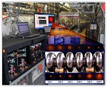
A novel technique known as in-situ plasma processing is helping scientists get more neutrons and better data for their experiments at the Spallation Neutron Source at the Department of Energy's Oak Ridge National Laboratory.
"Plasma cleaning is a well-known technique in electrostatics," said ORNL's Research Accelerator Division Director Kevin Jones, "but it has not been applied before to superconducting cavities, and there are some interesting tricks that you have to develop and apply in order to make it all work."
SNS's linear accelerator, or linac, features a set of 20-plus cryomodules--large, barrel-shaped capsules, necessary for focusing and accelerating the proton beam. Inside each cryomodule are 3-4 niobium cavity strings, accordion-like components bathed in liquid helium that keeps the cavities cold to aid in generating very strong electrical fields that drive the beam's acceleration.
Jones explained that over the years trace amounts of hydrocarbon contamination builds up inside the niobium cavities, lessening their ability to sustain high electrical fields, and thus decreasing the beam's potential energy. The conventional response to the problem would be to physically take the cryomodules offline, disassemble them, remove the contamination using ultra-pure water or a chemical rinse, and then finally put everything back together--a labor intensive and costly process.
ORNL staff scientist Marc Doleans and postdoctoral researcher Puneet Tyagi found a better solution. Together they led a team of technicians from SNS's Superconducting Linac Systems Group that undertook a program of rigorous surface science and bench-top experiments with room-temperature cavities that culminated in a series of trial procedures using an offline, spare cryomodule.
"Essentially what they're doing is using hot plasma to burn off the hydrocarbons on and just below the surfaces [inside the niobium cavities]. They're using an inert gas with a few percent of oxygen. Basically, the oxygen gobbles up all the bad atoms off the surface of the niobium, and afterwards everything gets pumped out as a gas," Jones said. "It's just cleaning off junk on the surface--kind of like polishing your car."
After the trial procedures were complete, the team tested the cryomodule's performance and saw a significant improvement. That gave the go ahead for the team to carry out the in-situ procedure in the accelerator tunnel during the facility's scheduled winter maintenance outage.
As expected, the procedure was a success. Not only did the team do in 3 weeks what would have taken 6 to 8 months using conventional methods, but furthermore, subsequent testing recorded an energy gain of 11 million electron volts (MeV). The increase from 938 to 949 MeV is a big step forward, according to Jones.
In addition to a few other upgrades, he said, "Today we're running the accelerator at the highest beam energy ever in neutron production at 957 MeV. If we use this procedure on, say, 5 more cryomodules, and we get equivalent gains, we can easily get up to operating at our design energy of 1,000 MeV."
Ramping up the power to the SNS proton beam enables the production of more neutrons for the thousands of scientists who visit the DOE Office of Science User Facility to conduct research.
The work is already generating a lot of buzz, and it's being viewed very positively, Jones says. In addition to their recent publication in the scientific journals NIM A and Applied Surface Science, the team has been asked to collaborate with other national labs conducting research into superconducting accelerators.
"This is high-profile stuff," Jones said. "It saves us an enormous amount of money, effort, and time in improving the performance of those cavities, and our investment has been worth every penny."
Share on:


Testimonial
"Our marketing partnership with I-Connect007 is already delivering. Just a day after our press release went live, we received a direct inquiry about our updated products!"
Rachael Temple - AlltematedSuggested Items
Driving Innovation: Depth Routing Processes—Achieving Unparalleled Precision in Complex PCBs
09/08/2025 | Kurt Palmer -- Column: Driving InnovationIn PCB manufacturing, the demand for increasingly complex and miniaturized designs continually pushes the boundaries of traditional fabrication methods, including depth routing. Success in these applications demands not only on robust machinery but also sophisticated control functions. PCB manufacturers rely on advanced machine features and process methodologies to meet their precise depth routing goals. Here, I’ll explore some crucial functions that empower manufacturers to master complex depth routing challenges.
Polar Instruments Announces Additive Transmission Line Support for Si9000e
08/20/2025 | Polar InstrumentsTransmission lines embedded into the PCB surface are a feature of UHDI constructions. The 2025 fall release of Polar's Si9000e PCB impedance & insertion loss transmission line field solver incorporates eight new single ended, differential and coplanar transmission line structures.
Henniker Plasma Launches Stratus Turnkey Plasma Manufacturing Cell
08/13/2025 | Henniker PlasmaHenniker Plasma, a leading manufacturer of plasma treatment systems, proudly announces the launch of its Stratus Plasma Manufacturing Cell range — a fully integrated, turnkey solution that combines advanced atmospheric plasma surface treatment with robotic automation.
Trouble in Your Tank: Metallizing Flexible Circuit Materials—Mitigating Deposit Stress
08/04/2025 | Michael Carano -- Column: Trouble in Your TankMetallizing materials, such as polyimide used for flexible circuitry and high-reliability multilayer printed wiring boards, provide a significant challenge for process engineers. Conventional electroless copper systems often require pre-treatments with hazardous chemicals or have a small process window to achieve uniform coverage without blistering. It all boils down to enhancing the adhesion of the thin film of electroless copper to these smooth surfaces.
Designers Notebook: Basic PCB Planning Criteria—Establishing Design Constraints
07/22/2025 | Vern Solberg -- Column: Designer's NotebookPrinted circuit board development flows more smoothly when all critical issues are predefined and understood from the start. As a basic planning strategy, the designer must first consider the product performance criteria, then determine the specific industry standards or specifications that the product must meet. Planning also includes a review of all significant issues that may affect the product’s manufacture, performance, reliability, overall quality, and safety.