


 Dan’s Biz Bookshelf: Four Important Books You Need to Read (Not Just Say You Have)
 The Marketing Minute: Cracking the Code of Technical Marketing


How Electrons Travel Through Exotic New Material
March 11, 2016 | Princeton UniversityEstimated reading time: 2 minutes
Researchers at Princeton University have observed a bizarre behavior in a strange new crystal that could hold the key for future electronic technologies. Unlike most materials in which electrons travel on the surface, in these new materials the electrons sink into the depths of the crystal through special conductive channels.
"It is like these electrons go down a rabbit hole and show up on the opposite surface," said Ali Yazdani, the Class of 1909 Professor of Physics. "You don't find anything else like this in other materials."
The research was published in the journal Science.
Yazdani and his colleagues discovered the odd behavior while studying electrons in a crystal made of layers of tantalum and arsenic. The material, called a Weyl semi-metal, behaves both like a metal, which conducts electrons, and an insulator, which blocks them. A better understanding of these and other "topological" materials someday could lead to new, faster electronic devices.
The team's experimental results suggest that the surface electrons plunge into the crystal only when traveling at a certain speed and direction of travel called the Weyl momentum, said Yazdani. "It is as if you have an electron on one surface, and it is cruising along, and when it hits some special value of momentum, it sinks into the crystal and appears on the opposite surface," he said.
These special values of momentum, also called Weyl points, can be thought of as portals where the electrons can depart from the surface and be conducted to the opposing surface. The theory predicts that the points come in pairs, so that a departing electron will make the return trip through the partner point.
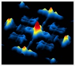
The team decided to explore the behavior of these electrons following research, published in Science last year by another Princeton team and separately by two independent groups, revealing that electrons in Weyl semi-metals are quite unusual. For example, their experiments implied that while most surface electrons create a wave pattern that resembles the spreading rings that ripple out when a stone is thrown into a pond, the surface electrons in the new materials should make only a half circle, earning them the name "Fermi arcs."
To get a more direct look at the patterns of electron flow in Weyl semi-metals, postdoctoral researcher Hiroyuki Inoue and graduate student András Gyenis in Yazdani's lab, with help from graduate student Seong Woo Oh, used a highly sensitive instrument called a scanning tunneling microscope, one of the few tools that can observe electron waves on a crystal surface. They obtained the tantalum arsenide crystals from graduate student Shan Jiang and assistant professor Ni Ni at the University of California-Los Angeles.
The results were puzzling. "Some of the interference patterns that we expected to see were missing," Yazdani said.
To help explain the phenomenon, Yazdani consulted B. Andrei Bernevig, associate professor of physics at Princeton, who has expertise in the theory of topological materials and whose group was involved in the first predictions of Weyl semi-metals in a 2015 paper published in Physical Review X.
Bernevig, with help from postdoctoral researchers Jian Li and Zhijun Wang, realized that the observed pattern made sense if the electrons in these unusual materials were sinking into the bulk of the crystal. "Nobody had predicted that there would be signals of this type of transport from a scanning tunneling microscope, so it came as a bit of a surprise," said Bernevig.
The next step, said Bernevig, is to look for the behavior in other crystals.
Share on:


Testimonial
"Our marketing partnership with I-Connect007 is already delivering. Just a day after our press release went live, we received a direct inquiry about our updated products!"
Rachael Temple - AlltematedSuggested Items
Curing and Verification in PCB Shadow Areas
09/17/2025 | Doug Katze, DymaxDesign engineers know a simple truth that often complicates electronics manufacturing: Light doesn’t go around corners. In densely populated PCBs, adhesives and coatings often fail to fully cure in shadowed regions created by tall ICs, connectors, relays, and tight housings.
Marcy’s Musings: Advancing the Advanced Materials Discussion
09/17/2025 | Marcy LaRont -- Column: Marcy's MusingsAs the industry’s most trusted global source of original content about the electronics supply chain, we continually ask you about your concerns, what you care about, and what you most want to learn about. Your responses are insightful and valuable. Thank you for caring enough to provide useful feedback and engage in dialogue.
September 2025 PCB007 Magazine: The Future of Advanced Materials
09/16/2025 | I-Connect007 Editorial TeamMoore’s Law is no more, and the advanced material solutions being developed to grapple with this reality are surprising, stunning, and perhaps a bit daunting. Buckle up for a dive into advanced materials and a glimpse into the next chapters of electronics manufacturing.
I-Connect007 Launches Advanced Electronics Packaging Digest
09/15/2025 | I-Connect007I-Connect007 is pleased to announce the launch of Advanced Electronics Packaging Digest (AEPD), a new monthly digital newsletter dedicated to one of the most critical and rapidly evolving areas of electronics manufacturing: advanced packaging at the interconnect level.
Panasonic Industry will Double the Production Capacity of MEGTRON Multi-layer Circuit Board Materials Over the Next Five Years
09/15/2025 | Panasonic Industry Co., Ltd.Panasonic Industry Co., Ltd., a Panasonic Group company, announced plans for a major expansion of its global production capacity for MEGTRON multi-layer circuit board materials today. The company plans to double its production over the next five years to meet growing demand in the AI server and ICT infrastructure markets.