


 Dan’s Biz Bookshelf: Four Important Books You Need to Read (Not Just Say You Have)
 The Marketing Minute: Cracking the Code of Technical Marketing


Atomic Vibrations in Nanomaterials
March 11, 2016 | ETH ZurichEstimated reading time: 2 minutes
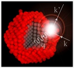
Researchers at ETH have shown for the first time what happens to atomic vibrations when materials are nanosized and how this knowledge can be used to systematically engineer nanomaterials for different applications.
All materials are made up of atoms, which vibrate. These vibrations, or "phonons", are responsible, for example, for how electric charge and heat is transported in materials. Vibrations of metals, semiconductors, and insulators in are well studied; however, now materials are being nanosized to bring better performance to applications such as displays, sensors, batteries, and catalytic membranes. What happens to vibrations when a material is nanosized has until now not been understood.
Soft Surfaces Vibrate Strongly
In a recent publication in Nature, ETH Professor Vanessa Wood and her colleagues explain what happens to atomic vibrations when materials are nanosized and how this knowledge can be used to systematically engineer nanomaterials for different applications.
The paper shows that when materials are made smaller than about 10 to 20 nanometers - that is, 5,000 times thinner than a human air – the vibrations of the outermost atomic layers on surface of the nanoparticle are large and play an important role in how this material behaves.
“For some applications, like catalysis, thermoelectrics, or superconductivity, these large vibrations may be good, but for other applications like LEDs or solar cells, these vibrations are undesirable,” explains Wood.
Indeed, the paper explains why nanoparticle-based solar cells have until now not met their full promise. The researchers showed using both experiment and theory that surface vibrations interact with electrons to reduce the photocurrent in solar cells.
“Now that we have proven that surface vibrations are important, we can systematically design materials to suppress or enhance these vibrations,” say Wood.
Improving Solar Cells
Wood’s research group has worked for a long time on a particular type of nanomaterial – colloidal nanocrystals – semiconductors with a diameter of 2 to 10 nanometers. These materials are interesting because their optical and electrical properties are dependent on their size, which can be easily changed during their synthesis.
These materials are now used commercially as red- and green-light emitters in LED-based TVs and are being explored as possible materials for low cost, solution-processed solar cells. Researchers have noticed that placing certain atoms around the surface of the nanocrystal can improve the performance of solar cells. The reason why this worked had not been understood. The work published in the Nature paper now gives the answer: a hard shell of atoms can suppress the vibrations and their interaction with electrons. This means a higher photocurrent and a higher efficiency solar cell.
Big Science to Study the Nanoscale
Experiments were conducted in Professor Wood’s labs at ETH Zurich and at the Swiss Spallation Neutron Source at the Paul Scherrer Institute. By observing how neutrons scatter off atoms in a material, it is possible to quantify how atoms in a material vibrate. To understand the neutron measurements, simulations of the atomic vibrations were run at the Swiss National Supercomputing Center (CSCS) in Lugano. Wood says, “without access to these large facilities, this work would not have been possible. We are incredibly fortunate here in Switzerland to have these world class facilities.”
Share on:


Testimonial
"Advertising in PCB007 Magazine has been a great way to showcase our bare board testers to the right audience. The I-Connect007 team makes the process smooth and professional. We’re proud to be featured in such a trusted publication."
Klaus Koziol - atgSuggested Items
Curing and Verification in PCB Shadow Areas
09/17/2025 | Doug Katze, DymaxDesign engineers know a simple truth that often complicates electronics manufacturing: Light doesn’t go around corners. In densely populated PCBs, adhesives and coatings often fail to fully cure in shadowed regions created by tall ICs, connectors, relays, and tight housings.
Marcy’s Musings: Advancing the Advanced Materials Discussion
09/17/2025 | Marcy LaRont -- Column: Marcy's MusingsAs the industry’s most trusted global source of original content about the electronics supply chain, we continually ask you about your concerns, what you care about, and what you most want to learn about. Your responses are insightful and valuable. Thank you for caring enough to provide useful feedback and engage in dialogue.
September 2025 PCB007 Magazine: The Future of Advanced Materials
09/16/2025 | I-Connect007 Editorial TeamMoore’s Law is no more, and the advanced material solutions being developed to grapple with this reality are surprising, stunning, and perhaps a bit daunting. Buckle up for a dive into advanced materials and a glimpse into the next chapters of electronics manufacturing.
I-Connect007 Launches Advanced Electronics Packaging Digest
09/15/2025 | I-Connect007I-Connect007 is pleased to announce the launch of Advanced Electronics Packaging Digest (AEPD), a new monthly digital newsletter dedicated to one of the most critical and rapidly evolving areas of electronics manufacturing: advanced packaging at the interconnect level.
Panasonic Industry will Double the Production Capacity of MEGTRON Multi-layer Circuit Board Materials Over the Next Five Years
09/15/2025 | Panasonic Industry Co., Ltd.Panasonic Industry Co., Ltd., a Panasonic Group company, announced plans for a major expansion of its global production capacity for MEGTRON multi-layer circuit board materials today. The company plans to double its production over the next five years to meet growing demand in the AI server and ICT infrastructure markets.