


 Dan’s Biz Bookshelf: Four Important Books You Need to Read (Not Just Say You Have)
 The Marketing Minute: Cracking the Code of Technical Marketing


Researchers Develop New Lens for Terahertz Radiation
March 15, 2016 | Brown UniversityEstimated reading time: 3 minutes
Terahertz radiation is a relatively unexplored slice of the electromagnetic spectrum, but it holds the promise of countless new imaging applications as well as wireless communication networks with extremely high bandwidth. The problem is that there are few off-the-shelf components available for manipulating terahertz waves.
Now, researchers from Brown University’s School of Engineering have developed a new type of lens for focusing terahertz radiation (which spans from about 100 to 10,000 GHz). The lens, made from an array of stacked metal plates with spaces between them, performs as well or better than existing terahertz lenses, and the architecture used to build the device could set the stage for a range of other terahertz components that don’t currently exist.
The work was led by Rajind Mendis, assistant professor of engineering (research) at Brown, who worked with Dan Mittleman, professor of engineering at Brown. The work is described in the journal Nature Scientific Reports.
“Any photonic system that uses terahertz – whether it’s in imaging, wireless communications or something else – will require lenses,” said Dan Mittleman, professor of engineering at Brown and the senior author on the new paper. “We wanted to look for new ways to focus terahertz radiation.”
Most lenses use the refractive properties of a material to focus light energy. Eyeglasses, for example, use convex glass to bend visible light and focus it on a certain spot. But for this new terahertz lens, the properties of the materials used don’t matter as much as the way in which the materials are arranged.
“It’s the architecture here that’s important,” Mendis said.
The new device is made from 32 metal plates, each 100 microns thick, with a 1-millimeter space between each plate. The plates have semicircular notches of different sizes cut out of one edge, such that when stacked horizontally the notches form a three-dimensional divot on one side of the device. When a terahertz beam enters the input side of the device, slices of the beam travel through the spaces between the plates. The concave output side of the device bends the beam slices to varying degrees such that the slices are all focused on a certain point.
Using the configuration developed for this new study, the researchers were able to focus a two-centimeter-diameter terahertz beam down to a four-millimeter spot. The radiation transmission through the device – the amount of radiation that makes it through the spaces as opposed to reflected back toward the source or dissipated inside the device – was about 80 percent. That’s significantly better than silicon lenses, which typically have a transmission loss of about 50 percent, and about the same as lenses made from Teflon.
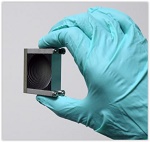
The image shows a a two-centimeter beam focused to four millimeters.
Mittleman lab / Brown University
Page 1 of 2
Share on:


Testimonial
"In a year when every marketing dollar mattered, I chose to keep I-Connect007 in our 2025 plan. Their commitment to high-quality, insightful content aligns with Koh Young’s values and helps readers navigate a changing industry. "
Brent Fischthal - Koh YoungSuggested Items
Knocking Down the Bone Pile: Best Practices for Electronic Component Salvaging
09/17/2025 | Nash Bell -- Column: Knocking Down the Bone PileElectronic component salvaging is the practice of recovering high-value devices from PCBs taken from obsolete or superseded electronic products. These components can be reused in new assemblies, reducing dependence on newly purchased parts that may be costly or subject to long lead times.
ICAPE Group Unveils Exclusive Report on Sustainability in Electronics Manufacturing
09/15/2025 | ICAPE GroupICAPE Group, a global leader in printed circuit boards (PCBs) and custom electronics manufacturing, today announces the launch of its 2025 Industry Outlook & Innovation Report: Sustainability in Electronics Manufacturing. This exclusive report is accompanied by fresh insights from a dedicated Statista survey of 100 electronics manufacturing professionals, commissioned by ICAPE Group.
Advanced Packaging-to-Board-Level Integration: Needs and Challenges
09/15/2025 | Devan Iyer and Matt Kelly, Global Electronics AssociationHPC data center markets now demand components with the highest processing and communication rates (low latencies and high bandwidth, often both simultaneously) and highest capacities with extreme requirements for advanced packaging solutions at both the component level and system level. Insatiable demands have been projected for heterogeneous compute, memory, storage, and data communications. Interconnect has become one of the most important pillars of compute for these systems.
Smart Automation: Odd-form Assembly—Dedicated Insertion Equipment Matters
09/09/2025 | Josh Casper -- Column: Smart AutomationLarge, irregular, or mechanically unique parts, often referred to as odd-form components, have never truly disappeared from electronics manufacturing. While many in the industry have been pursuing miniaturization, faster placement speeds, and higher-density PCBs, certain market sectors are moving in the opposite direction.
Talking with Tamara: Floor Planning Policies
09/04/2025 | Andy Shaughnessy, Design007 MagazineTamara Jovanovic is an electrical engineer with Masimo, a medical equipment manufacturer. She’s been designing PCBs for seven years and earned a master’s degree in electrical engineering in 2022. I asked Tamara to share her thoughts on floor planning—the challenges, techniques, and advice for designers setting up floor planning strategies.