


 Dan’s Biz Bookshelf: Four Important Books You Need to Read (Not Just Say You Have)
 The Marketing Minute: Cracking the Code of Technical Marketing


3D-printed Antenna
March 17, 2016 | ESAEstimated reading time: 1 minute
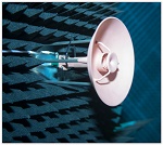
A prototype 3D-printed antenna being put to work in ESA’s Compact Antenna Test Facility, a shielded chamber for antenna and radio-frequency testing.
“This is the Agency’s first 3D-printed dual-reflector antenna,” explains engineer Maarten van der Vorst, who designed it.
“Incorporating a corrugated feedhorn and two reflectors, it has been printed all-in-one in a polymer, then plated with copper to meet its radio-frequency (RF) performance requirements.
“Designed for future mega-constellation small satellite platforms, it would need further qualification to make it suitable for real space missions, but at this stage we’re most interested in the consequences on RF performance of the low-cost 3D-printing process.”
“Although the surface finish is rougher than for a traditionally manufactured antenna, we’re very happy with the resulting performance,” says antenna test engineer Luis Rolo.
“We have a very good agreement between the measurements and the simulations. Making a simulation based on a complete 3D model of the antenna leads to a significant increase in its accuracy.
“By using this same model to 3D print it in a single piece, any source of assembly misalignments and errors are removed, enabling such excellent results.”
Two different antennas were produced by Swiss company SWISSto12, employing a special copper-plating technique to coat the complex shapes.
“As a next step, we aim at more complex geometries and target higher frequencies,” adds Maarten, a member of ESA’s Electromagnetics & Space Environment Division. “And eventually we want to build space-qualified RF components for Earth observation and science instruments.”
Based at ESA’s ESTEC technical centre in Noordwijk, the Netherlands, the test range is isolated from outside electromagnetic radiation while its inside walls are covered with ‘anechoic’ foam to absorb radio signals, simulating infinite space.
The range is part of ESA’s suite of antenna testing facilities, intended for smaller antennas and subsystems, with larger antennas and entire satellites put to the test in its ‘big brother’, the Hertz chamber.
Share on:


Testimonial
"The I-Connect007 team is outstanding—kind, responsive, and a true marketing partner. Their design team created fresh, eye-catching ads, and their editorial support polished our content to let our brand shine. Thank you all! "
Sweeney Ng - CEE PCBSuggested Items
Electrodeposited Copper Foils Market to Grow by $11.7 Billion Over 2025-2032
09/18/2025 | Globe NewswireThe global electrodeposited copper foils market is poised for dynamic growth, driven by the rising adoption in advanced electronics and renewable energy storage solutions.
MacDermid Alpha Showcases Advanced Interconnect Solutions at PCIM Asia 2025
09/18/2025 | MacDermid Alpha Electronics SolutionsMacDermid Alpha Electronic Solutions, a global leader in materials for power electronics and semiconductor assembly, will showcase its latest interconnect innovations in electronic interconnect materials at PCIM Asia 2025, held from September 24 to 26 at the Shanghai New International Expo Centre, Booth N5-E30
Trouble in Your Tank: Implementing Direct Metallization in Advanced Substrate Packaging
09/15/2025 | Michael Carano -- Column: Trouble in Your TankDirect metallization systems based on conductive graphite are gaining popularity throughout the world. The environmental and productivity gains achievable with this process are outstanding. Direct metallization reduces the costs of compliance, waste treatment, and legal issues related to chemical exposure. A graphite-based direct plate system has been devised to address these needs.
Closing the Loop on PCB Etching Waste
09/09/2025 | Shawn Stone, IECAs the PCB industry continues its push toward greener, more cost-efficient operations, Sigma Engineering’s Mecer System offers a comprehensive solution to two of the industry’s most persistent pain points: etchant consumption and rinse water waste. Designed as a modular, fully automated platform, the Mecer System regenerates spent copper etchants—both alkaline and acidic—and simultaneously recycles rinse water, transforming a traditionally linear chemical process into a closed-loop system.
Driving Innovation: Depth Routing Processes—Achieving Unparalleled Precision in Complex PCBs
09/08/2025 | Kurt Palmer -- Column: Driving InnovationIn PCB manufacturing, the demand for increasingly complex and miniaturized designs continually pushes the boundaries of traditional fabrication methods, including depth routing. Success in these applications demands not only on robust machinery but also sophisticated control functions. PCB manufacturers rely on advanced machine features and process methodologies to meet their precise depth routing goals. Here, I’ll explore some crucial functions that empower manufacturers to master complex depth routing challenges.