


 Dan’s Biz Bookshelf: Four Important Books You Need to Read (Not Just Say You Have)
 The Marketing Minute: Cracking the Code of Technical Marketing


Recent Advances in Optical Materials
March 18, 2016 | ACN NewswireEstimated reading time: 1 minute
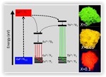
Japanese scientists have reviewed recent progress in advanced optical materials based on gadolinium aluminate garnet (GAG), while pointing out the knowledge gaps that need to be filled to improve their optical performance.
Their article, published in the open access journal Science and Technology of Advanced Materials, investigates the conditions in which GAG materials perform best. GAG is a synthetic material used in optics and crystal growth, as seeds to grow large crystals of similar materials.
Rare-earth aluminate garnets are an important family of multi-functional ceramic materials. They are useful in phosphors and lasers - often with medical applications such as cancer diagnosis and treatment. Researchers have tried to improve the chemical stability and luminescence of these materials and to understand their novel emission features.
In their review, Ji-Guang Li and Yoshio Sakka, of Japan's National Institute for Materials Science, discuss the ways to stabilise the GAG lattice and its performance in scintillators and "down-conversion phosphors", where high-energy photons are converted to low-energy ones.
Anti-site defects, where atoms of different types exchange their positions, are common in these materials. These can have profound effects on emissions as the atoms interact with excited electrons. This needs to be better understood, say the authors, in order to improve the overall performance of this class of optical materials.
Share on:


Testimonial
"Advertising in PCB007 Magazine has been a great way to showcase our bare board testers to the right audience. The I-Connect007 team makes the process smooth and professional. We’re proud to be featured in such a trusted publication."
Klaus Koziol - atgSuggested Items
Curing and Verification in PCB Shadow Areas
09/17/2025 | Doug Katze, DymaxDesign engineers know a simple truth that often complicates electronics manufacturing: Light doesn’t go around corners. In densely populated PCBs, adhesives and coatings often fail to fully cure in shadowed regions created by tall ICs, connectors, relays, and tight housings.
Marcy’s Musings: Advancing the Advanced Materials Discussion
09/17/2025 | Marcy LaRont -- Column: Marcy's MusingsAs the industry’s most trusted global source of original content about the electronics supply chain, we continually ask you about your concerns, what you care about, and what you most want to learn about. Your responses are insightful and valuable. Thank you for caring enough to provide useful feedback and engage in dialogue.
September 2025 PCB007 Magazine: The Future of Advanced Materials
09/16/2025 | I-Connect007 Editorial TeamMoore’s Law is no more, and the advanced material solutions being developed to grapple with this reality are surprising, stunning, and perhaps a bit daunting. Buckle up for a dive into advanced materials and a glimpse into the next chapters of electronics manufacturing.
I-Connect007 Launches Advanced Electronics Packaging Digest
09/15/2025 | I-Connect007I-Connect007 is pleased to announce the launch of Advanced Electronics Packaging Digest (AEPD), a new monthly digital newsletter dedicated to one of the most critical and rapidly evolving areas of electronics manufacturing: advanced packaging at the interconnect level.
Panasonic Industry will Double the Production Capacity of MEGTRON Multi-layer Circuit Board Materials Over the Next Five Years
09/15/2025 | Panasonic Industry Co., Ltd.Panasonic Industry Co., Ltd., a Panasonic Group company, announced plans for a major expansion of its global production capacity for MEGTRON multi-layer circuit board materials today. The company plans to double its production over the next five years to meet growing demand in the AI server and ICT infrastructure markets.