Matrix's NEW Hakuto Dry Film Laminator Impresses at IPC
April 14, 2016 | MatrixEstimated reading time: 1 minute

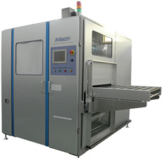
Matrix is delighted with customer reaction at last month’s North American IPC unveiling of the new Hakuto Mach 630NP/6630NP Series Dry Film Laminators and is now ready to provide Sales and Service to all regions of North America.
During the recent APEX/IPC Show in Las Vegas, customers were amazed at the new and Innovative technology such as changing rolls in a matter of seconds.
Matrix believes the NEW Hakuto Mach 630NP Dry Film Laminator will change the game for PCB manufacturing.
Fred Long, Matrix Business Development says: “The new Mach 630NP machine addresses the accuracy needed to assist in the transfer of very fine lines on the latest HSLL laminates using Super Low Profile Copper surfaces. This is made possible by the new Lamination Module with its EVEN Heat and EVEN Pressure across the entire surface of the laminated panel. In addition, the ability to change the rubber lamination rolls in seconds will not only increase productivity but will also offer alternative “quick change” rubber solutions for different product needs. The complete redesign of the film lamination approach will now begin to reach the most important users of this latest technology. Matrix is eager to show manufacturers that by using the new system, Productivity and Yield will now surpass all traditional ROI expectations.”
See the PCB007 IPC Interview with Dan Feinberg and Fred Long discussing the new laminating machine and its innovative features, click here.
During the next few weeks, Matrix is scheduled to place additional machines in three specific regional areas in the US. Customers will then be able to travel to these sites and see the machines in operation.
About Matrix USA Inc.
Committed to the motto, “Quality Products, Dependable People”, Matrix was established in 1977 with the objective of providing quality raw materials to the North American Printed Circuit Board Industry. Matrix has four rapid-response warehouses located throughout the US and Canada that fulfill high quality, fast delivery, and custom orders daily. For further information, click here.
Testimonial
"Our marketing partnership with I-Connect007 is already delivering. Just a day after our press release went live, we received a direct inquiry about our updated products!"
Rachael Temple - AlltematedSuggested Items
Trouble in Your Tank: Implementing Direct Metallization in Advanced Substrate Packaging
09/15/2025 | Michael Carano -- Column: Trouble in Your TankDirect metallization systems based on conductive graphite are gaining popularity throughout the world. The environmental and productivity gains achievable with this process are outstanding. Direct metallization reduces the costs of compliance, waste treatment, and legal issues related to chemical exposure. A graphite-based direct plate system has been devised to address these needs.
Closing the Loop on PCB Etching Waste
09/09/2025 | Shawn Stone, IECAs the PCB industry continues its push toward greener, more cost-efficient operations, Sigma Engineering’s Mecer System offers a comprehensive solution to two of the industry’s most persistent pain points: etchant consumption and rinse water waste. Designed as a modular, fully automated platform, the Mecer System regenerates spent copper etchants—both alkaline and acidic—and simultaneously recycles rinse water, transforming a traditionally linear chemical process into a closed-loop system.
Driving Innovation: Depth Routing Processes—Achieving Unparalleled Precision in Complex PCBs
09/08/2025 | Kurt Palmer -- Column: Driving InnovationIn PCB manufacturing, the demand for increasingly complex and miniaturized designs continually pushes the boundaries of traditional fabrication methods, including depth routing. Success in these applications demands not only on robust machinery but also sophisticated control functions. PCB manufacturers rely on advanced machine features and process methodologies to meet their precise depth routing goals. Here, I’ll explore some crucial functions that empower manufacturers to master complex depth routing challenges.
Trouble in Your Tank: Minimizing Small-via Defects for High-reliability PCBs
08/27/2025 | Michael Carano -- Column: Trouble in Your TankTo quote the comedian Stephen Wright, “If at first you don’t succeed, then skydiving is not for you.” That can be the battle cry when you find that only small-diameter vias are exhibiting voids. Why are small holes more prone to voids than larger vias when processed through electroless copper? There are several reasons.
The Government Circuit: Navigating New Trade Headwinds and New Partnerships
08/25/2025 | Chris Mitchell -- Column: The Government CircuitAs global trade winds continue to howl, the electronics manufacturing industry finds itself at a critical juncture. After months of warnings, the U.S. Government has implemented a broad array of tariff increases, with fresh duties hitting copper-based products, semiconductors, and imports from many nations. On the positive side, tentative trade agreements with Europe, China, Japan, and other nations are providing at least some clarity and counterbalance.