


 Dan’s Biz Bookshelf: Four Important Books You Need to Read (Not Just Say You Have)
 The Marketing Minute: Cracking the Code of Technical Marketing


Using Nanotubes to Create Single Photons for Quantum Communication
April 13, 2016 | U.S. Department of EnergyEstimated reading time: 1 minute
The Science
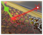
Critical information, ranging from credit card numbers to national security data, is sent in streams of light, or laser pulses. However, the data transmitted in this manner can be stolen by splitting out a few photons (packets of light) from the laser pulse. Such eavesdropping could be prevented by encoding the data into single photons. But that requires generating single photons. Researchers demonstrated a new material, made from tiny carbon tubes, that emits the desired photons at room temperature.
The Impact
Digital eavesdropping could be prevented by encoding bits of information in the properties, or quantum mechanical states, of single photons. Single photons emitted by carbon nanotubes altered, or doped with oxygen, are especially attractive for realizing this quantum information technology.
Summary
Single photon generation requires an isolated, quantum mechanical, two-level system that can emit only one photon in one excitation-emission cycle. While artificial nanoscale materials (such as quantum dots and vacancy centers in diamonds) have been explored for single photon generation, none have emerged as the ideal candidate that meets all of the technological requirements. These requirements include the ability to generate single photons in the 1.3 to 1.5 µm fiber optic telecommunication wavelength range at room temperature. Earlier studies revealed that carbon nanotubes were not suited for use in quantum communications because the tubes required extremely low temperatures and had strong photoluminescence fluctuations. In contrast to these earlier findings, researchers led by Han Htoon and Stephen Doorn of the Center for Integrated Nanotechnologies showed that oxygen doping of carbon nanotubes can lead to fluctuation-free photoluminescence emission in the telecommunication wavelength range. Experiments measuring the time-distribution of two successive photon emission events also unambiguously demonstrated single photon emission at room temperature. Furthermore, because oxygen doping is achieved through a simple deposition of a silicon dioxide layer, these doped carbon nanotubes are fully compatible with silicon microfabrication technology and can be fabricated into electrically driven single photon sources. In addition, the silicon dioxide layer encapsulating the nanotubes allows for their easy integration into electronic and photonic integrated circuits. Beyond the implementation of this new method into quantum communication technologies, nanotube-based single photon sources could enable other transformative quantum technologies, including ultra-sensitive absorption measurements, sub-diffraction imaging, and linear quantum computing.
Share on:


Testimonial
"The I-Connect007 team is outstanding—kind, responsive, and a true marketing partner. Their design team created fresh, eye-catching ads, and their editorial support polished our content to let our brand shine. Thank you all! "
Sweeney Ng - CEE PCBSuggested Items
MEMS & Imaging Sensors Summit to Spotlight Sensing Revolution for Europe’s Leadership
09/11/2025 | SEMIIndustry experts will gather November 19-20 at the SEMI MEMS & Imaging Sensors Summit 2025 to explore the latest breakthroughs in AI-driven MEMS and imaging optimization, AR/VR technologies, and advanced sensor solutions for critical defence applications.
Direct Imaging System Market Size to Hit $4.30B by 2032, Driven by Increasing Demand for High-Precision PCB Manufacturing
09/11/2025 | Globe NewswireAccording to the SNS Insider, “The Direct Imaging System Market size was valued at $2.21 Billion in 2024 and is projected to reach $4.30 Billion by 2032, growing at a CAGR of 8.68% during 2025-2032.”
I-Connect007’s Editor’s Choice: Five Must-Reads for the Week
07/04/2025 | Marcy LaRont, I-Connect007For our industry, we have seen several bullish market announcements over the past few weeks, including one this week by IDC on the massive growth in the global server market. We’re also closely watching global trade and nearshoring. One good example of successful nearshoring is Rehm Thermal Systems, which celebrates its 10th anniversary in Mexico and the official opening of its new building in Guadalajara.
Driving Innovation: Direct Imaging vs. Conventional Exposure
07/01/2025 | Simon Khesin -- Column: Driving InnovationMy first camera used Kodak film. I even experimented with developing photos in the bathroom, though I usually dropped the film off at a Kodak center and received the prints two weeks later, only to discover that some images were out of focus or poorly framed. Today, every smartphone contains a high-quality camera capable of producing stunning images instantly.
United Electronics Corporation Advances Manufacturing Capabilities with Schmoll MDI-ST Imaging Equipment
06/24/2025 | United Electronics CorporationUnited Electronics Corporation has successfully installed the advanced Schmoll MDI-ST (XL) imaging equipment at their advanced printed circuit board facility. This significant technology investment represents a continued commitment to delivering superior products and maintaining their position as an industry leader in precision PCB manufacturing.