


 Dan’s Biz Bookshelf: Four Important Books You Need to Read (Not Just Say You Have)
 The Marketing Minute: Cracking the Code of Technical Marketing


'Odd Couple' Monolayer Semiconductors Align to Advance Optoelectronics
April 16, 2016 | ORNLEstimated reading time: 3 minutes
Epitaxy, or growing crystalline film layers that are templated by a crystalline substrate, is a mainstay of manufacturing transistors and semiconductors. If the material in one deposited layer is the same as the material in the next layer, it can be energetically favorable for strong bonds to form between the highly ordered, perfectly matched layers. In contrast, trying to layer dissimilar materials is a great challenge if the crystal lattices don’t match up easily. Then, weak van der Waals forces create attraction but don’t form strong bonds between unlike layers.
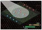
In a study led by the Department of Energy’s Oak Ridge National Laboratory, scientists synthesized a stack of atomically thin monolayers of two lattice-mismatched semiconductors. One, gallium selenide, is a “p-type” semiconductor, rich in charge carriers called “holes.” The other, molybdenum diselenide, is an “n-type” semiconductor, rich in electron charge carriers. Where the two semiconductor layers met, they formed an atomically sharp heterostructure called a p–n junction, which generated a photovoltaic response by separating electron–hole pairs that were generated by light. The achievement of creating this atomically thin solar cell, published in Science Advances, shows the promise of synthesizing mismatched layers to enable new families of functional two-dimensional (2D) materials.
The idea of stacking different materials on top of each other isn’t new by itself. In fact, it is the basis for most electronic devices in use today. But such stacking usually only works when the individual materials have crystal lattices that are very similar, i.e., they have a good “lattice match.” This is where this research breaks new ground by growing high-quality layers of very different 2D materials, broadening the number of materials that can be combined and thus creating a wider range of potential atomically thin electronic devices.
“Because the two layers had such a large lattice mismatch between them, it’s very unexpected that they would grow on each other in an orderly way,” said ORNL’s Xufan Li, lead author of the study. “But it worked.”
The group was the first to show that monolayers of two different types of metal chalcogenides—binary compounds of sulfur, selenium or tellurium with a more electropositive element or radical—having such different lattice constants can be grown together to form a perfectly aligned stacking bilayer. “It’s a new, potential building block for energy-efficient optoelectronics,” Li said.
Upon characterizing their new bilayer building block, the researchers found that the two mismatched layers had self-assembled into a repeating long-range atomic order that could be directly visualized by the Moiré patterns they showed in the electron microscope. “We were surprised that these patterns aligned perfectly,” Li said.
Researchers in ORNL’s Functional Hybrid Nanomaterials group, led by David Geohegan, conducted the study with partners at Vanderbilt University, the University of Utah and Beijing Computational Science Research Center.
“These new 2D mismatched layered heterostructures open the door to novel building blocks for optoelectronic applications,” said senior author Kai Xiao of ORNL. “They can allow us to study new physics properties which cannot be discovered with other 2D heterostructures with matched lattices. They offer potential for a wide range of physical phenomena ranging from interfacial magnetism, superconductivity and Hofstadter’s butterfly effect.”
Li first grew a monolayer of molybdenum diselenide, and then grew a layer of gallium selenide on top. This technique, called “van der Waals epitaxy,” is named for the weak attractive forces that hold dissimilar layers together. “With van der Waals epitaxy, despite big lattice mismatches, you can still grow another layer on the first,” Li said. Using scanning transmission electron microscopy, the team characterized the atomic structure of the materials and revealed the formation of Moiré patterns.
The scientists plan to conduct future studies to explore how the material aligns during the growth process and how material composition influences properties beyond the photovoltaic response. The research advances efforts to incorporate 2D materials into devices.
For many years, layering different compounds with similar lattice cell sizes has been widely studied. Different elements have been incorporated into the compounds to produce a wide range of physical properties related to superconductivity, magnetism and thermoelectrics. But layering 2D compounds having dissimilar lattice cell sizes is virtually unexplored territory.
“We’ve opened the door to exploring all types of mismatched heterostructures,” Li said.
The title of the paper is “Two-dimensional GaSe/MoSe2 misfit bilayer heterojunctions by van der Waals epitaxy.”
Research, including materials synthesis, was supported by the DOE Office of Science. Materials characterization was conducted in part at the Center for Nanophase Materials Sciences, a DOE Office of Science User Facility at ORNL. ORNL Laboratory Directed Research and Development funds supported some of the device measurements in the study.
Share on:


Testimonial
"We’re proud to call I-Connect007 a trusted partner. Their innovative approach and industry insight made our podcast collaboration a success by connecting us with the right audience and delivering real results."
Julia McCaffrey - NCAB GroupSuggested Items
Curing and Verification in PCB Shadow Areas
09/17/2025 | Doug Katze, DymaxDesign engineers know a simple truth that often complicates electronics manufacturing: Light doesn’t go around corners. In densely populated PCBs, adhesives and coatings often fail to fully cure in shadowed regions created by tall ICs, connectors, relays, and tight housings.
Marcy’s Musings: Advancing the Advanced Materials Discussion
09/17/2025 | Marcy LaRont -- Column: Marcy's MusingsAs the industry’s most trusted global source of original content about the electronics supply chain, we continually ask you about your concerns, what you care about, and what you most want to learn about. Your responses are insightful and valuable. Thank you for caring enough to provide useful feedback and engage in dialogue.
September 2025 PCB007 Magazine: The Future of Advanced Materials
09/16/2025 | I-Connect007 Editorial TeamMoore’s Law is no more, and the advanced material solutions being developed to grapple with this reality are surprising, stunning, and perhaps a bit daunting. Buckle up for a dive into advanced materials and a glimpse into the next chapters of electronics manufacturing.
I-Connect007 Launches Advanced Electronics Packaging Digest
09/15/2025 | I-Connect007I-Connect007 is pleased to announce the launch of Advanced Electronics Packaging Digest (AEPD), a new monthly digital newsletter dedicated to one of the most critical and rapidly evolving areas of electronics manufacturing: advanced packaging at the interconnect level.
Panasonic Industry will Double the Production Capacity of MEGTRON Multi-layer Circuit Board Materials Over the Next Five Years
09/15/2025 | Panasonic Industry Co., Ltd.Panasonic Industry Co., Ltd., a Panasonic Group company, announced plans for a major expansion of its global production capacity for MEGTRON multi-layer circuit board materials today. The company plans to double its production over the next five years to meet growing demand in the AI server and ICT infrastructure markets.