


 Dan’s Biz Bookshelf: Four Important Books You Need to Read (Not Just Say You Have)
 The Marketing Minute: Cracking the Code of Technical Marketing


Team Builds First Quantum Cascade Laser on Silicon
April 21, 2016 | The Optical SocietyEstimated reading time: 2 minutes
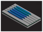
A team of researchers from across the country, led by Alexander Spott, University of California, Santa Barbara, USA, have built the first quantum cascade laser on silicon. The advance may have applications that span from chemical bond spectroscopy and gas sensing, to astronomy and free-space communications.
Integrating lasers directly on silicon chips is challenging, but it is much more efficient and compact than coupling external laser light to the chips. The indirect bandgap of silicon makes it difficult to build a laser out of silicon, but diode lasers can be built with III-V materials such as InP or GaAs. By directly bonding an III-V layer on top of the silicon wafer and then using the III-V layers to generate gain for the laser, this same group has integrated a multiple quantum well laser on silicon that operates at 2 µm. Limitations in diode lasers prevent going to longer wavelengths where there are many more applications, so the group turned their attention to using quantum cascade lasers instead.
Building a quantum cascade laser on silicon was a challenging task made more difficult by the fact that silicon dioxide becomes heavily absorptive at longer wavelengths in the mid-infrared.
"This meant that not only did we have to build a different type of laser on silicon, we had to build a different silicon waveguide too," Spott explained. "We built a type of waveguide called a SONOI waveguide [silicon-on-nitride-on-insulator], which uses a layer of silicon nitride [SiN] underneath the silicon waveguide, rather than just SiO2."
The breakthrough could lead to several applications, Spott explained. Traditionally, silicon photonic devices operate at near-infrared wavelengths, with applications in data transmission and telecommunications. However, there is emerging research interest in building these silicon photonic devices for longer mid-infrared wavelengths, for a range of sensing and detection applications, such as chemical bond spectroscopy, gas sensing, astronomy, oceanographic sensing, thermal imaging, explosive detection, and free-space communications.
The next step for the team is to improve the heat dissipation to improve the performance of these QCLs and to allow them to make continuous-wave QCLs on silicon. "We generally hope to improve the design to get higher powers and efficiency," Spott said. "This brings us closer to building fully integrated mid-infrared devices on a silicon chip, such as spectrometers or gas sensors. Silicon is inexpensive, the fabrication can be scaled up to significantly reduce the cost of individual chips, and many small devices can be built on the same silicon chip for example multiple different types of sensors operating at different mid-infrared wavelengths."
Share on:


Testimonial
"We’re proud to call I-Connect007 a trusted partner. Their innovative approach and industry insight made our podcast collaboration a success by connecting us with the right audience and delivering real results."
Julia McCaffrey - NCAB GroupSuggested Items
MEMS & Imaging Sensors Summit to Spotlight Sensing Revolution for Europe’s Leadership
09/11/2025 | SEMIIndustry experts will gather November 19-20 at the SEMI MEMS & Imaging Sensors Summit 2025 to explore the latest breakthroughs in AI-driven MEMS and imaging optimization, AR/VR technologies, and advanced sensor solutions for critical defence applications.
Direct Imaging System Market Size to Hit $4.30B by 2032, Driven by Increasing Demand for High-Precision PCB Manufacturing
09/11/2025 | Globe NewswireAccording to the SNS Insider, “The Direct Imaging System Market size was valued at $2.21 Billion in 2024 and is projected to reach $4.30 Billion by 2032, growing at a CAGR of 8.68% during 2025-2032.”
I-Connect007’s Editor’s Choice: Five Must-Reads for the Week
07/04/2025 | Marcy LaRont, I-Connect007For our industry, we have seen several bullish market announcements over the past few weeks, including one this week by IDC on the massive growth in the global server market. We’re also closely watching global trade and nearshoring. One good example of successful nearshoring is Rehm Thermal Systems, which celebrates its 10th anniversary in Mexico and the official opening of its new building in Guadalajara.
Driving Innovation: Direct Imaging vs. Conventional Exposure
07/01/2025 | Simon Khesin -- Column: Driving InnovationMy first camera used Kodak film. I even experimented with developing photos in the bathroom, though I usually dropped the film off at a Kodak center and received the prints two weeks later, only to discover that some images were out of focus or poorly framed. Today, every smartphone contains a high-quality camera capable of producing stunning images instantly.
United Electronics Corporation Advances Manufacturing Capabilities with Schmoll MDI-ST Imaging Equipment
06/24/2025 | United Electronics CorporationUnited Electronics Corporation has successfully installed the advanced Schmoll MDI-ST (XL) imaging equipment at their advanced printed circuit board facility. This significant technology investment represents a continued commitment to delivering superior products and maintaining their position as an industry leader in precision PCB manufacturing.