


 Dan’s Biz Bookshelf: Four Important Books You Need to Read (Not Just Say You Have)
 The Marketing Minute: Cracking the Code of Technical Marketing


Cooling Graphene-based Film Close to Pilot-scale Production
April 29, 2016 | CHALMERS UNIVERSITY OF TECHNOLOGYEstimated reading time: 1 minute
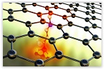
Heat dissipation in electronics and optoelectronics is a severe bottleneck in the further development of systems in these fields. To come to grips with this serious issue, researchers at Chalmers University of Technology have developed an efficient way of cooling electronics by using functionalized graphene nanoflakes. The results will be published in the renowned journal Nature Communications.
"Essentially, we have found a golden key with which to achieve efficient heat transport in electronics and other power devices by using graphene nanoflake-based film. This can open up potential uses of this kind of film in broad areas, and we are getting closer to pilot-scale production based on this discovery," says Johan Liu, Professor of Electronics Production at Chalmers University of Technology in Sweden.
The researchers studied the heat transfer enhancement of the film with different functionalized amino-based and azide-based silane molecules, and found that the heat transfer efficiency of the film can be improved by over 76 percent by introducing functionalization molecules, compared to a reference system without the functional layer. This is mainly because the contact resistance was drastically reduced by introducing the functionalization molecules.
Meanwhile, molecular dynamic simulations and ab initio calculations reveal that the functional layer constrains the cross-plane scattering of low-frequency phonons, which in turn enhances in-plane heat-conduction of the bonded film by recovering the long flexural phonon lifetime. The results suggested potential thermal management solutions for electronic devices.
In the research, scientists studied a number of molecules that were immobilized at the interfaces and at the edge of graphene nanoflake-based sheets forming covalent bonds. They also probed interface thermal resistance by using a photo-thermal reflectance measurement technique to demonstrate an improved thermal coupling due to functionalization.
"This is the first time that such systematic research has been done. The present work is much more extensive than previously published results from several involved partners, and it covers more functionalization molecules and also more extensive direct evidence of the thermal contact resistance measurement," says Johan Liu.
Share on:


Testimonial
"We’re proud to call I-Connect007 a trusted partner. Their innovative approach and industry insight made our podcast collaboration a success by connecting us with the right audience and delivering real results."
Julia McCaffrey - NCAB GroupSuggested Items
Electrodeposited Copper Foils Market to Grow by $11.7 Billion Over 2025-2032
09/18/2025 | Globe NewswireThe global electrodeposited copper foils market is poised for dynamic growth, driven by the rising adoption in advanced electronics and renewable energy storage solutions.
Breakthrough in Non-Contact Solder Removal Earns Kurtz Ersa 2025 Mexico Technology Award at SMTA Guadalajara
09/18/2025 | Kurtz Ersa Inc.Kurtz Ersa Inc., a leading supplier of electronics production equipment, is proud to announce that it has been awarded a 2025 Mexico Technology Award in the category of Rework & Repair for its HR 600P Automatic Rework System.
A.R.T. Invests in Latest Equipment to Further Enhance Electronics Training Facilities
09/17/2025 | A.R.T. Ltd.Advanced Rework Technology Ltd. (A.R.T.), a leading independent IPC-accredited training provider, has announced a series of new equipment investments at its state-of-the-art training centre.
Richardson Electronics Appoints Daniel Albers to Drive Made-in-USA Contract Manufacturing Expansion
09/17/2025 | Globe NewswireRichardson Electronics, Ltd., a global provider of engineered solutions for the green energy, power management, and custom display markets, announced the appointment of Daniel Albers to spearhead business development for its expanded, Made-in-USA contract manufacturing efforts.
STMicroelectronics to Advance Next-generation Chip Manufacturing Technology with New PLP Pilot Line in Tours, France
09/17/2025 | STMicroelectronicsSTMicroelectronics, a global semiconductor leader serving customers across the spectrum of electronics applications, today announced new details regarding the development of the next generations of Panel-Level Packaging (PLP) technology through a pilot line in its Tours site, France, which is expected to be operational in Q3 2026.