


 Dan’s Biz Bookshelf: Four Important Books You Need to Read (Not Just Say You Have)
 The Marketing Minute: Cracking the Code of Technical Marketing


Sustainable Nanotechnology
May 3, 2016 | DTUEstimated reading time: 2 minutes
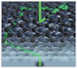
Corrosion protection with graphene
In a world where at least 3 % of the GDP of developed countries are being used to protect against or rebuild after corrosion, better barrier materials would make a large impact, prolonging the life time for the objects exposed to corrosion and reducing the consumption of resources.
Since its isolation in 2004, graphene has drawn huge attention due to its unique electrical properties, but more recently its mechanical and chemical properties are being more heavily investigated. Single layers of graphene are impermeable even for molecules as small as hydrogen, making graphene the perfect barrier.
When graphene protective coatings are taken out of the lab, however, things are less perfect. Even though graphene is the strongest material known relative to its size, a single atomic layer of any material is still easily damaged. When metal, graphene and a corrosive liquid are exposed at the same time, an electrochemical process called galvanic corrosion can in some cases even enhance the corrosion rate – and this may only show up after extended durations of time.
“However,” PhD Student Adam Stoot says “we can grow graphene directly on a catalytic metal surface, and when we use nickel, the graphene typically forms relatively thick coatings – with hundreds of layers. Even a 100 nm thick coating with 300 layers is still extremely thin compared to conventional, micrometre thick coatings for corrosion protection”.
Researchers from DTU Nanotech in collaboration with SP Group A/S have grown such multilayer graphene coatings and have proved longer term performance of graphene coatings in highly corrosive boiling saline solutions. An effective and also conducting coating can have a profound impact in several application areas such as fuel cells, batteries, sensors and contacts.
Test chip with several CZTS solar cells and their metal contacts. Cell thickness is 2 micrometres.
Thin film solar cells
In solar cells, the materials responsible for converting sunlight into electricity are semiconductors. In those materials, first, electrons have to overcome a moderate energy gap by exploiting the energy of sunlight, and then, they can contribute to the electric current in the solar cell.
The current standard solar cell semiconductor, silicon, has an energy gap of the indirect type. As predicted by quantum mechanics, an indirect gap allows only weak absorption of light. Therefore, silicon needs to be at least 200 micrometres thick to absorb all sunlight. On the other hand, sulphur based semiconductor compounds such as Cu2ZnSnS4 (CZTS) or Cu2SnS3 (CTS) have an energy gap of the direct type. They absorb light more than 200 times better than silicon and their thickness can be cut down to 0.8 micrometres, thus saving a lot of resources. For this reason, we call them "thin-film solar cells".
Still, the actual laboratory efficiency of CZTS and CTS is mostly below 10%, whereas silicon excels with 25% in large scale production. PhD student Andrea Crovetto explains that “to improve the efficiency, we need to address a major challenge with these materials, namely the phase purity. Because there are many chemical elements involved in those compound semiconductors, we have to find synthesis methods that result in the correct, pure material with fairly large crystals so that crystal defects and loss of light-excited electrons are reduced”.
Share on:


Testimonial
"The I-Connect007 team is outstanding—kind, responsive, and a true marketing partner. Their design team created fresh, eye-catching ads, and their editorial support polished our content to let our brand shine. Thank you all! "
Sweeney Ng - CEE PCBSuggested Items
Curing and Verification in PCB Shadow Areas
09/17/2025 | Doug Katze, DymaxDesign engineers know a simple truth that often complicates electronics manufacturing: Light doesn’t go around corners. In densely populated PCBs, adhesives and coatings often fail to fully cure in shadowed regions created by tall ICs, connectors, relays, and tight housings.
Marcy’s Musings: Advancing the Advanced Materials Discussion
09/17/2025 | Marcy LaRont -- Column: Marcy's MusingsAs the industry’s most trusted global source of original content about the electronics supply chain, we continually ask you about your concerns, what you care about, and what you most want to learn about. Your responses are insightful and valuable. Thank you for caring enough to provide useful feedback and engage in dialogue.
September 2025 PCB007 Magazine: The Future of Advanced Materials
09/16/2025 | I-Connect007 Editorial TeamMoore’s Law is no more, and the advanced material solutions being developed to grapple with this reality are surprising, stunning, and perhaps a bit daunting. Buckle up for a dive into advanced materials and a glimpse into the next chapters of electronics manufacturing.
I-Connect007 Launches Advanced Electronics Packaging Digest
09/15/2025 | I-Connect007I-Connect007 is pleased to announce the launch of Advanced Electronics Packaging Digest (AEPD), a new monthly digital newsletter dedicated to one of the most critical and rapidly evolving areas of electronics manufacturing: advanced packaging at the interconnect level.
Panasonic Industry will Double the Production Capacity of MEGTRON Multi-layer Circuit Board Materials Over the Next Five Years
09/15/2025 | Panasonic Industry Co., Ltd.Panasonic Industry Co., Ltd., a Panasonic Group company, announced plans for a major expansion of its global production capacity for MEGTRON multi-layer circuit board materials today. The company plans to double its production over the next five years to meet growing demand in the AI server and ICT infrastructure markets.