


 Dan’s Biz Bookshelf: Four Important Books You Need to Read (Not Just Say You Have)
 The Marketing Minute: Cracking the Code of Technical Marketing


New Fabrication and Thermo-Optical Tuning of Whispering Gallery Microlasers
May 4, 2016 | OISTEstimated reading time: 2 minutes
Scientists from the Light-Matter Interactions Unit, led by Professor Síle Nic Chormaic at the Okinawa Institute of Science and Technology Graduate University (OIST), have developed a new technique to fabricate glass microlasers and tune them using compressed air. The new technique, published in Scientific Reports, could pave the way for the simple serial production of glass microlasers and could be used in a wide range of applications, such as optical communications, chemical or biosensing.
Microlasers are tiny optical devices a few tens of micrometres in diameter that are able to create intense light with only one colour or wavelength. OIST researchers found a new method to fabricate a special type of glass microlaser, called whispering gallery microlasers. Whispering gallery microlasers are doughnut-shaped or spherical devices produced from glass doped with rare earth elements, such as erbium or ytterbium (Er or Yb). Inside the microlasers, light is reflected over and over creating a 10-100 metre long optical path within a tiny device that’s the size of a grain of sand.
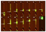
Left: The green fluorescence shows light trapped around the circular cavity, displaying the whispering gallery effect. Right: Laser light collected from the microlaser shows only a single color or wavelength.
Taking advantage of the different melting temperatures of silica and Er or Yb doped phosphate glass, OIST scientists have devised a new way to produce microlasers via glass wetting, or glass-on-glass fabrication. In this new technique, a strand of Er or Yb doped phosphate glass is melted and allowed to flow around a hollow capillary of silica. This is possible because of the different melting temperatures of silica and phosphate glass at 1500°C and 500°C, respectively. This technique produces bottle-shaped microlasers, which are 170 micrometres in diameter. The bottle-shape can then be modified to become a thin coating of only a few micrometres in diameter around the capillary.
The new glass wetting technique to fabricate microlasers. A phosphate glass wire doped with ytterbium and erbium (Er:Yb, with melting temperature of 500°C) is melted and allowed to flow around a hollow silica capillary (melting temperature of 1500°C).
A thin coating (around one micron thick) is formed on the capillary. Laser light can be created at almost any point on the capillary, indicated by the white arrow. The thin coating allows for the fabrication of much smaller microlasers.
While fabricating doped glass microlasers using traditional methods can be tedious, with each individual sphere being attached to a glass strand, this glass wetting technique allows scientists to make any number of microlasers quickly and in series.
This technique also facilitates a new way of tuning the wavelength or colour of light emitted by the microlasers. The tuning is achieved by a combination of pressure and temperature. Compressed gas passed through the capillary cools the walls of the hollow structure. This cooling effect makes the diameter of the microlaser contract, which changes the laser output wavelength.
Microlasers prepared with this new technique were used to measure the air flow in microfluidic devices and have been shown to be more sensitive than commercial electronic flow sensors, as well as 10,000 times smaller.
“We wanted the ability to tune micro-scale lasers without increasing the size and the complexity of the device and keeping high quality,” points out Dr Jonathan Ward, the first author of this study. “This could be a step towards the quick and easy fabrication of smaller devices for biosensing and optical communications.”
Share on:


Testimonial
"We’re proud to call I-Connect007 a trusted partner. Their innovative approach and industry insight made our podcast collaboration a success by connecting us with the right audience and delivering real results."
Julia McCaffrey - NCAB GroupSuggested Items
Curing and Verification in PCB Shadow Areas
09/17/2025 | Doug Katze, DymaxDesign engineers know a simple truth that often complicates electronics manufacturing: Light doesn’t go around corners. In densely populated PCBs, adhesives and coatings often fail to fully cure in shadowed regions created by tall ICs, connectors, relays, and tight housings.
VIDEOTON EAS's Bulgarian Subsidiary Expands Into Automotive Products
09/15/2025 | VideotonVEAS Bulgaria, engaged in electronics manufacturing, has joined the ranks of VIDEOTON companies authorized to produce automotive products.
Dymax Mexico to Showcase Light-Curing Technologies at SMTA Guadalajara Expo & Tech Forum 2025
09/05/2025 | DymaxDymax, a global manufacturer of rapid light-curing materials and equipment, will participate in SMTA Guadalajara Expo & Tech Forum, taking place September 17-18, 2025, at the Guadalajara Expo Center in Guadalajara, Jalisco, Mexico.
September 2025 SMT007 Magazine: An Eye on India
09/02/2025 | I-Connect007 Editorial TeamIndia is on track to become the world’s fastest-growing major economy within the next two years, and that momentum is already reshaping its electronics manufacturing sector. Whether you work with Indian suppliers or serve Indian customers, chances are the country will become a bigger part of your supply chain in the near future.
AiM Future, Franklin Wireless Sign MOU to Jointly Develop Lightweight AI Model and High-Efficiency 1 TOPS AI SoC Chipset
09/01/2025 | BUSINESS WIREAiM Future, a leading AI semiconductor design company, has signed a Memorandum of Understanding (MOU) with Franklin Wireless Corp., a global leader in intelligent wireless solutions, to jointly develop a lightweight AI model and a high-efficiency 1 TOPS performance AI SoC chipset.