


 Dan’s Biz Bookshelf: Four Important Books You Need to Read (Not Just Say You Have)
 The Marketing Minute: Cracking the Code of Technical Marketing


Molybdenum Disulfide Holds Promise for Light Absorption
May 6, 2016 | Rice UniversityEstimated reading time: 1 minute
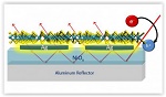
Mechanics know molybdenum disulfide (MoS2) as a useful lubricant in aircraft and motorcycle engines and in the CV and universal joints of trucks and automobiles. Rice University engineering researcher Isabell Thomann knows it as a remarkably light-absorbent substance that holds promise for the development of energy-efficient optoelectronic and photocatalytic devices.
“Basically, we want to understand how much light can be confined in an atomically thin semiconductor monolayer of MoS2,” said Thomann, assistant professor of electrical and computer engineering and of materials science and nanoengineering and of chemistry. “By using simple strategies, we were able to absorb 35 to 37 percent of the incident light in the 400- to 700-nanometer wavelength range, in a layer that is only 0.7 nanometers thick.”
Thomann and Rice graduate students Shah Mohammad Bahauddin and Hossein Robatjazi have recounted their findings in a paper titled “Broadband Absorption Engineering To Enhance Light Absorption in Monolayer MoS2,” which was recently published in the American Chemical Society journal ACS Photonics. The research has many applications, including development of efficient and inexpensive photovoltaic solar panels.
“Squeezing light into these extremely thin layers and extracting the generated charge carriers is an important problem in the field of two-dimensional materials,” she said. “That’s because monolayers of 2-D materials have different electronic and catalytic properties from their bulk or multilayer counterparts.”
Thomann and her team used a combination of numerical simulations, analytical models and experimental optical characterizations. Using three-dimensional electromagnetic simulations, they found that light absorption was enhanced 5.9 times compared with using MoS2 on a sapphire substrate.
“If light absorption in these materials was perfect, we’d be able to create all sorts of energy-efficient optoelectronic and photocatalytic devices. That’s the problem we’re trying to solve,” Thomann said.
She is pleased with her lab’s progress but concedes that much work remains to be done. “The goal, of course, is 100 percent absorption, and we’re not there yet.”
The research was supported by the National Science Foundation and the Welch Foundation.
Share on:


Testimonial
"In a year when every marketing dollar mattered, I chose to keep I-Connect007 in our 2025 plan. Their commitment to high-quality, insightful content aligns with Koh Young’s values and helps readers navigate a changing industry. "
Brent Fischthal - Koh YoungSuggested Items
Curing and Verification in PCB Shadow Areas
09/17/2025 | Doug Katze, DymaxDesign engineers know a simple truth that often complicates electronics manufacturing: Light doesn’t go around corners. In densely populated PCBs, adhesives and coatings often fail to fully cure in shadowed regions created by tall ICs, connectors, relays, and tight housings.
Marcy’s Musings: Advancing the Advanced Materials Discussion
09/17/2025 | Marcy LaRont -- Column: Marcy's MusingsAs the industry’s most trusted global source of original content about the electronics supply chain, we continually ask you about your concerns, what you care about, and what you most want to learn about. Your responses are insightful and valuable. Thank you for caring enough to provide useful feedback and engage in dialogue.
September 2025 PCB007 Magazine: The Future of Advanced Materials
09/16/2025 | I-Connect007 Editorial TeamMoore’s Law is no more, and the advanced material solutions being developed to grapple with this reality are surprising, stunning, and perhaps a bit daunting. Buckle up for a dive into advanced materials and a glimpse into the next chapters of electronics manufacturing.
I-Connect007 Launches Advanced Electronics Packaging Digest
09/15/2025 | I-Connect007I-Connect007 is pleased to announce the launch of Advanced Electronics Packaging Digest (AEPD), a new monthly digital newsletter dedicated to one of the most critical and rapidly evolving areas of electronics manufacturing: advanced packaging at the interconnect level.
Panasonic Industry will Double the Production Capacity of MEGTRON Multi-layer Circuit Board Materials Over the Next Five Years
09/15/2025 | Panasonic Industry Co., Ltd.Panasonic Industry Co., Ltd., a Panasonic Group company, announced plans for a major expansion of its global production capacity for MEGTRON multi-layer circuit board materials today. The company plans to double its production over the next five years to meet growing demand in the AI server and ICT infrastructure markets.