


 Dan’s Biz Bookshelf: Four Important Books You Need to Read (Not Just Say You Have)
 The Marketing Minute: Cracking the Code of Technical Marketing


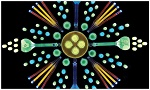
Quantum Dots by Nature
May 10, 2016 | Lehigh UniversityEstimated reading time: 5 minutes
Lehigh researchers have successfully demonstrated the first precisely controlled, biological way to manufacture quantum dots. This one-step method starts with engineered bacterial cells in a simple, aqueous solution and ends with functional semiconducting nanoparticles, all without resorting to high temperatures and toxic chemicals.
Born of an ideal collaboration among three Lehigh faculty researchers, this elegant technique has great potential for green manufacturing of quantum dots (QDs), which are used in transistors, solar cells, LEDs, lasers and medical imaging. Current industrial processes to produce them are messy, requiring toxic solvents, heat and high pressure.
Bryan Berger, associate professor of chemical and biomolecular engineering and bioengineering, wondered in 2012 whether the bacterial strain Stenotrophomonas maltophilia could be manipulated to generate QDs on command, since it had previously been known to exhibit heavy metal resistance.
Berger teamed up with colleagues Steve McIntosh, associate professor of chemical and biomolecular engineering and member of Lehigh’s Class of ’61; Chris Kiely, the Harold B. Chambers Senior Professor of Materials Science and Engineering; Robert Skibbens, professor of biological sciences; and Ivan Korendovych, assistant professor of chemistry at Syracuse University. Together they won a $2 million grant in 2013 from NSF’s Division of Emerging Frontiers in Research and Innovation (EFRI) to prove the production of cadmium sulfide QDs using an engineered form of Stenotrophomonas. They tailored the bacteria to grow nanocrystalline metal sulfides including QDs, building on earlier research, which was funded by Lehigh’s Faculty Innovation Grant (FIG) and Collaborative Research Opportunity Grant (CORE) programs.
“The beauty of a biological approach is that it cuts down on the production needs, environmental burden and production time quite a lot,” says Berger. Industrial processes take many hours to grow the nanocrystals, which then need to undergo additional processing and purifying steps. On the other hand, biosynthesis takes minutes to hours maximum to make the full range of quantum dot sizes (about 2 to 3 nanometers) in a continuous, environmentally friendly process at ambient conditions in water that needs no post-processing steps to harvest the final, water-soluble product. Because bacterial cells are much larger than the nanocrystals, researchers simply use a centrifuge to pull the cells away from the QDs in the solution.
More recently, the researchers have branched into creating lead sulfide QDs and are working on oxide-based materials, widening the range of QD practical applications. Their underlying technique allows them to control the particle size to fractions of a nanometer, an essential function, since particle size determines the QD’s optical and electronic properties.
Cell-based growth needs only basic equipment in a typical biochemistry wet lab setting. Using a process called directed evolution, researchers altered the bacteria so they would selectively produce quantum dots. Housed in a beaker containing water, cadmium and sulfur precursors, and minimum levels of carbon and nitrogen, the cells forgo most normal biological functions. They build quantum dots by sequestering metal ions from their environment, generating a reactive sulfur source and controlling the resultant structure to form a crystal.
Perfecting the methodology to structurally analyze individual nanoparticles required a highly sophisticated Scanning Transmission Electron Microscope (STEM). Lehigh’s Electron Microscopy and Nanofabrication Facility was able to provide a $4.5 million state-of-the-art instrument that allowed the researchers to examine the structure and composition of each QD, which is only composed of tens to hundreds of atoms.
“Even with this new microscope, we’re pushing the limits of what can be done,” says Kiely. The instrument scans an ultra-fine electron beam across a field of QDs. The atoms block the electrons in the beam, producing a kind of shadow image on a fluorescent screen, akin to the way an object blocking light produces a shadow on the wall. A digital camera records the highly magnified atomic resolution image of the nanocrystal for analysis.
Page 1 of 2
Share on:


Testimonial
"Advertising in PCB007 Magazine has been a great way to showcase our bare board testers to the right audience. The I-Connect007 team makes the process smooth and professional. We’re proud to be featured in such a trusted publication."
Klaus Koziol - atgSuggested Items
Electrodeposited Copper Foils Market to Grow by $11.7 Billion Over 2025-2032
09/18/2025 | Globe NewswireThe global electrodeposited copper foils market is poised for dynamic growth, driven by the rising adoption in advanced electronics and renewable energy storage solutions.
iDEAL Semiconductor Announces Polar Semiconductor as Manufacturing Partner for SuperQ™ Power Devices
09/18/2025 | PRNewswireiDEAL Semiconductor confirms that its ultra-efficient SuperQ™ silicon power devices are now in production at Polar Semiconductor, a leading foundry specializing in high-voltage, power, and sensor technologies.
U.S. Manufacturing Jobs Decline Amid Tariffs and Immigration Crackdown
09/17/2025 | I-Connect007 Editorial TeamManufacturers in the U.S. are cutting jobs even as President Donald Trump pushes policies he says will revitalize the industry. Employers shed 12,000 manufacturing jobs in August, while payrolls in the sector have fallen by 42,000 since April, according to a new analysis from the Center for American Progress (CAP) based on government labor data.
Richardson Electronics Appoints Daniel Albers to Drive Made-in-USA Contract Manufacturing Expansion
09/17/2025 | Globe NewswireRichardson Electronics, Ltd., a global provider of engineered solutions for the green energy, power management, and custom display markets, announced the appointment of Daniel Albers to spearhead business development for its expanded, Made-in-USA contract manufacturing efforts.
GlobalFoundries Joins World Economic Forum’s Global Lighthouse Network for Manufacturing Excellence
09/17/2025 | GlobalFoundriesGlobalFoundries announced that the World Economic Forum (WEF) has designated its 300mm fab in Singapore as part of the Global Lighthouse Network (GLN) of advanced manufacturers.