


 Dan’s Biz Bookshelf: Four Important Books You Need to Read (Not Just Say You Have)
 The Marketing Minute: Cracking the Code of Technical Marketing


New Electrical Energy Transmission System Makes Distance Wireless Charging a Reality
May 11, 2016 | Universitat Autònoma de BarcelonaEstimated reading time: 2 minutes
Wireless charging of mobile devices is possibly one of the most desired of technological milestones. Some devices already can be charged wirelessly by placing the mobile device on top of a charging base. The next step, charging devices without the need of taking them out of one’s pocket, might be just around the corner.
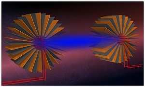
A group of researchers from the Department of Physics of Universitat Autònoma de Barcelona have developed a system which can efficiently transfer electrical energy between two separated circuits thanks to the use of metamaterials. This system is still in the experimental stage, but once it has been perfected and can be applied to mobile devices, it will be able to charge them wirelessly and at a longer distance than currently possible.
Today's wireless devices make use of induction to charge through a special case adapted to the device and a charging base connected to an electrical socket. When the device is placed on top of the base, this generates a magnetic field which induces an electric current inside the case and, without the need to use any cables, the device is charged. If the device is separated from the base, the energy is not transferred efficiently enough and the battery cannot be charged.
The system created by UAB researchers overcome these limitations. It is made up of metamaterials which combine layers of ferromagnetic materials, such as magnets, and conductor materials such as copper. The metamaterials envelop the emitter and receptor and enable transferring electrical energy between the two, at a distance and with unprecedented efficiency.
With the use of metamaterial crowns researchers were able in the lab to increase the transmission efficiency 35-fold, “and there is much more room for improvement, since theoretically the efficiency can be increased even more if conditions and the design of the experiment are perfected” explains Àlvar Sánchez, director of the research.
“Enveloping the two circuits with metamaterial crowns has the same effect as bringing them close together; it's as if the space between them literally disappears”, states Jordi Prat, lead author of the paper.
Moreover, the materials needed to construct these crowns such as copper and ferrite are easily available. The first experiments conducted with the aim of concentrating static magnetic fields required the use of superconductor metamaterials, unfeasible for everyday uses with mobile devices. “In contrast, low frequency electromagnetic waves - the ones used to transfer electrical energy from one circuit to the other - only need conventional conductors and magnets”, Carles Navau explains.
Published this week in Advanced Materials, the research was conducted by researchers from the Electromagnetism Group of the UAB Department of Physics Àlvar Sánchez (also an ICREA Acadèmia researcher) and Carles Navau, with the collaboration of Jordi Prat, currently researcher at the Institute for Quantum Optics and Quantum Information of the Austrian Academy of Sciences in Innsbruck.
The device has been patented by the UAB and several companies abroad have already showed interest in applying the technology to their products. The research was funded by the PRODUCTE project of the Government of Catalonia, the European Regional Development Fund (ERDF) and the Spanish Ministry for Economy and Competitiveness.
Share on:


Testimonial
"The I-Connect007 team is outstanding—kind, responsive, and a true marketing partner. Their design team created fresh, eye-catching ads, and their editorial support polished our content to let our brand shine. Thank you all! "
Sweeney Ng - CEE PCBSuggested Items
Electrodeposited Copper Foils Market to Grow by $11.7 Billion Over 2025-2032
09/18/2025 | Globe NewswireThe global electrodeposited copper foils market is poised for dynamic growth, driven by the rising adoption in advanced electronics and renewable energy storage solutions.
MacDermid Alpha Showcases Advanced Interconnect Solutions at PCIM Asia 2025
09/18/2025 | MacDermid Alpha Electronics SolutionsMacDermid Alpha Electronic Solutions, a global leader in materials for power electronics and semiconductor assembly, will showcase its latest interconnect innovations in electronic interconnect materials at PCIM Asia 2025, held from September 24 to 26 at the Shanghai New International Expo Centre, Booth N5-E30
Trouble in Your Tank: Implementing Direct Metallization in Advanced Substrate Packaging
09/15/2025 | Michael Carano -- Column: Trouble in Your TankDirect metallization systems based on conductive graphite are gaining popularity throughout the world. The environmental and productivity gains achievable with this process are outstanding. Direct metallization reduces the costs of compliance, waste treatment, and legal issues related to chemical exposure. A graphite-based direct plate system has been devised to address these needs.
Closing the Loop on PCB Etching Waste
09/09/2025 | Shawn Stone, IECAs the PCB industry continues its push toward greener, more cost-efficient operations, Sigma Engineering’s Mecer System offers a comprehensive solution to two of the industry’s most persistent pain points: etchant consumption and rinse water waste. Designed as a modular, fully automated platform, the Mecer System regenerates spent copper etchants—both alkaline and acidic—and simultaneously recycles rinse water, transforming a traditionally linear chemical process into a closed-loop system.
Driving Innovation: Depth Routing Processes—Achieving Unparalleled Precision in Complex PCBs
09/08/2025 | Kurt Palmer -- Column: Driving InnovationIn PCB manufacturing, the demand for increasingly complex and miniaturized designs continually pushes the boundaries of traditional fabrication methods, including depth routing. Success in these applications demands not only on robust machinery but also sophisticated control functions. PCB manufacturers rely on advanced machine features and process methodologies to meet their precise depth routing goals. Here, I’ll explore some crucial functions that empower manufacturers to master complex depth routing challenges.