


 Dan’s Biz Bookshelf: Four Important Books You Need to Read (Not Just Say You Have)
 The Marketing Minute: Cracking the Code of Technical Marketing


Reducing 30% Chip Area of STT-MRAM while Increasing Memory Bit Yield by 70%
May 17, 2016 | Tohoku UniversityEstimated reading time: 1 minute
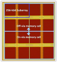
In a world first, researchers from Tohoku University have successfully developed a technology to stack magnetic tunnel junctions (MTJ) directly on the vertical interconnect access (via) without causing deterioration to its electric/magnetic characteristics. The via in an integrated circuit design is a small opening that allows a conductive connection between the different layers of a semiconductor device.
This new discovery will be particularly significant in reducing the chip area of spin-transfer torque magnetic random access memory (STT-MRAM), making its commercialization more practical.
The team led by Professor Tetsuo Endoh, Director of the Center for Innovative Integrated Electronic Systems (CIES), focused on reducing the memory cell area of STT-MRAMs in order to lower manufacturing costs, making them competitive with conventional semiconductor memories like dynamic random access memory (DRAM).
Because MTJs use magnetic properties, the quality of the surface between the MTJ and its lower electrode is important. If the surface area is not smooth, the electric/magnetic characteristics of the MTJ will degrade. For this reason, placing an MTJ directly on the via holes in STT-MRAMs has been avoided until now, although it increases the size of the memory cell.
Endoh's group has tackled the issue by developing a special polishing process technology to prevent any interference between the MTJ and its lower electrode. The technology's effectiveness was successfully verified by an experiment using single-MTJ test chips.
To further test the success of this development, a 2-Mbit STT-MRAM test chip integrating the new technology has been designed to verify the space needed for the integrated circuits -- this includes more than 1million MTJs.
"Not only does this test chip show a 70% improvement in its memory bit yield compared to standard STT-MRAM, but its memory cell area is reduced by 30%," says Endoh. "It will be very effective for reducing the chip area of MRAM."
CIES develops material, process, circuit and test technologies in integrated electronic systems. The center's main focus is on developing high-performance, low-power technologies for a more energy-efficient society.
Share on:


Testimonial
"In a year when every marketing dollar mattered, I chose to keep I-Connect007 in our 2025 plan. Their commitment to high-quality, insightful content aligns with Koh Young’s values and helps readers navigate a changing industry. "
Brent Fischthal - Koh YoungSuggested Items
Meet the Author Podcast: Martyn Gaudion Unpacks the Secrets of High-Speed PCB Design
07/16/2025 | I-Connect007In this special Meet the Author episode of the On the Line with… podcast, Nolan Johnson sits down with Martyn Gaudion, signal integrity expert, managing director of Polar Instruments, and three-time author in I-Connect007’s popular The Printed Circuit Designer’s Guide to... series.
Intervala Hosts Employee Car and Motorcycle Show, Benefit Nonprofits
08/27/2024 | IntervalaIntervala hosted an employee car and motorcycle show, aptly named the Vala-Cruise and it was a roaring success! Employees had the chance to show off their prized wheels, and it was incredible to see the variety and passion on display.
KIC Honored with IPC Recognition for 25 Years of Membership and Contributions to Electronics Manufacturing Industry
06/24/2024 | KICKIC, a renowned pioneer in thermal process and temperature measurement solutions for electronics manufacturing, is proud to announce that it has been recognized by IPC for 25 years of membership and significant contributions to electronics manufacturing.
Boeing Starliner Spacecraft Completes Successful Crewed Docking with International Space Station
06/07/2024 | BoeingNASA astronauts Barry "Butch" Wilmore and Sunita "Suni" Williams successfully docked Boeing's Starliner spacecraft to the International Space Station (ISS), about 26 hours after launching from Cape Canaveral Space Force Station.
KIC’s Miles Moreau to Present Profiling Basics and Best Practices at SMTA Wisconsin Chapter PCBA Profile Workshop
01/25/2024 | KICKIC, a renowned pioneer in thermal process and temperature measurement solutions for electronics manufacturing, announces that Miles Moreau, General Manager, will be a featured speaker at the SMTA Wisconsin Chapter In-Person PCBA Profile Workshop.