-

- News
- Books
Featured Books
- pcb007 Magazine
Latest Issues
Current Issue
Engineering Economics
The real cost to manufacture a PCB encompasses everything that goes into making the product: the materials and other value-added supplies, machine and personnel costs, and most importantly, your quality. A hard look at real costs seems wholly appropriate.
Alternate Metallization Processes
Traditional electroless copper and electroless copper immersion gold have been primary PCB plating methods for decades. But alternative plating metals and processes have been introduced over the past few years as miniaturization and advanced packaging continue to develop.
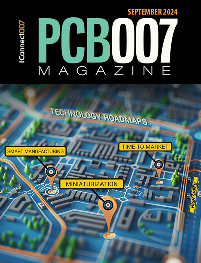
Technology Roadmaps
In this issue of PCB007 Magazine, we discuss technology roadmaps and what they mean for our businesses, providing context to the all-important question: What is my company’s technology roadmap?
- Articles
- Columns
Search Console
- Links
- Media kit
||| MENU - pcb007 Magazine
How the Giant Magnetoelectric Effect Occurs in Bismuth Ferrite
May 23, 2016 | MIPTEstimated reading time: 3 minutes
Suggested Items
Beyond Design: High-speed Rules of Thumb
11/21/2024 | Barry Olney -- Column: Beyond DesignThe idiom “rule of thumb” is often used in electronics design and has its origins in the practice of measuring roughly with one’s thumb. Rules of thumb are easy-to-remember, broadly accurate guides or principles based on practice rather than theory. They are used to help feed our intuition to find a quick solution based on experience. We are often forced to use rules of thumb in PCB design in the absence of expensive analysis tools. We also use them to get quick ballpark figures initially and then fine-tune the numbers with further analysis. We can use rules of thumb as a sanity check to assess whether we are using our tools correctly. In this month’s column, I will present some commonly used and helpful rules for high-speed PCB design.
ASMPT: Highly Flexible Die and Flip-chip Bonder for Co-packaged Optics Production
11/20/2024 | ASMPTThe high-precision AMICRA NANO die and flip-chip bonder has been specially developed for the production of co-packaged optics where which optical and electronic components are integrated in a common housing. With its exceptional process stability and a placement accuracy of ±0.2 μm @ 3 σ, this innovative bonding system is ideally equipped for the communication technology of the future.
SEMI Europe Recognizes Schneider Electric as a Leader in Diversity and Inclusion at SEMICON Europa 2024
11/14/2024 | SEMISEMI Europe and the SEMI European Advisory Council for Diversity and Inclusion announced Schneider Electric as the recipient of the 2023 SEMI Industry Leader in Diversity and Inclusion Award. Frederic Godemel, Executive Vice President, Power Systems and Services at Schneider Electric accepted the award presented at SEMICON Europa 2024 during the SEMI Networking Night Dinner.
Foxconn Strengthens Solid-State Battery Investment, Eyes Two-Wheeler Market as Testing Ground
11/12/2024 | TrendForceHon Hai subsidiary Foxconn has recently established Foxconn New Energy Battery (Zhengzhou) Co., Ltd. in Henan, China. The newly formed company will focus on battery manufacturing, sales, and R&D into automotive components.
Exploring Innovation Through Alternate Metals and Sputtering
11/11/2024 | Marcy LaRont, I-Connect007Dr. Evelyne Parmentier has a PhD in physical chemistry from ETH Zurich. She was born in Luxembourg and is now a proud resident of Switzerland, where she has been part of Dyconex’s R&D engineering team for the past two years. Evelyne gave a presentation at the EIPC Summer Conference titled “Functionalization of Printed Circuit Boards Through Introducing Alternate Metals Through Sputtered Layers,” where she asked her audience, “If there are 93 metals in the periodic table, why are we not using more of them?”

