


 Dan’s Biz Bookshelf: Four Important Books You Need to Read (Not Just Say You Have)
 The Marketing Minute: Cracking the Code of Technical Marketing


New Tabletop Instrument Tests Electron Mobility for Next-generation Electronics
May 25, 2016 | AIP.orgEstimated reading time: 3 minutes
The National High Magnetic Field Laboratory, with facilities in Florida and New Mexico, offers scientists access to enormous machines that create record-setting magnetic fields. The strong magnetic fields help researchers probe the fundamental structure of materials to better understand and manipulate their properties. Yet large-scale facilities like the MagLab are scarce, and scientists must compete with others for valuable time on the machines.
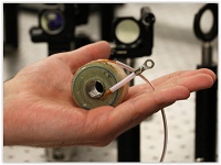
Now researchers from the United Kingdom, in collaboration with industry partners from Germany, have built a tabletop instrument that can perform measurements that were only previously possible at large national magnet labs. The measurements will help in the development of next generation electronic devices employing 2-D materials, said Ben Spencer, a post-doctoral research associate working in Darren Graham's group at the University of Manchester's Photon Science Institute, who helped develop the new instrument.
The researchers describe their work in a paper in the journal Applied Physics Letters, from AIP Publishing.
Since the 1950s, experiments conducted with magnetic fields have played a pivotal role in the development of semiconductors devices -- like transistors and light-emitting diodes -- that have changed the world.
One magnetic field technique is called cyclotron resonance. In a magnetic field, the charged particles in a material start to move in circles around the magnetic field lines. The orbiting particles interact with light differently depending on properties like their mass, concentration, and on how easily they move through the material. By shining light on the material in the magnetic field and recording what frequency and how much light is absorbed, scientists can learn important information about how easily charged particles move, a critical property in electronic devices.
One of the main obstacles to wide-spread use of cyclotron resonance is that some materials require an extremely high magnetic field to get the charged particles to move fast enough to interact with the light.
Recently researchers created a small, high-powered magnet that can generate fields of around 30 Tesla, about 600,000 times stronger than the Earth's magnetic field and 20 times stronger than the MRI scanners typically used in hospitals.
The new magnet is compact enough for a tabletop machine, yet the magnet can only generate a field in short pulses that each last for a fleeting one-hundredth of a second.
"The challenge in doing cyclotron resonance with these pulsed magnets is being able to record your data within the brief time period that the magnet is on," Spencer said. "The breakthrough we have made is in the measurement technique."
Spencer and his colleagues used an approach called an asynchronous optical sampling technique to increase the number of measurements during one pulse to around 100. Previous experiments with a similar magnet system were limited to four measurements per pulse.
The team worked with researchers from Laser Quantum, a laser manufacturer, to incorporate ultrafast lasers into the new instrument. The "Taccor" lasers they used run at repetition rates of 1 billion cycles per second, more than 10 times higher than the typical repetition rates for ultrafast laser systems, Spencer said. The fast laser allowed data acquisition times on the order of one ten-thousandth of a second, which meant up to a hundred measurements could be taken during the transient magnet pulse.
"It is this leap forward that will now enable routine cyclotron resonance measurements on a tabletop in a laboratory environment," Spencer said.
The team tested their system by measuring the properties of electrons at the interface of the two semiconductors AlGaN and GaN. Such interfaces could form an important part of new, energy-saving transistors.
"This work is feeding into a programme of work at Cambridge University on developing AlGaN/GaN-based high electron mobility transistors. These promise much lower power consumption than current devices, which will ultimately lead to energy savings in a wide range of consumer electronic devices. We are also starting to investigate a range of other two-dimensional materials using this instrument, including the new wonder 2-D material graphene," Graham said.
Ultimately, the team hopes their new instrument could facilitate rapid progress in many areas of semiconductor device development. The system can be easily moved to different universities, and it makes it easy to think of a measurement, and simply perform it the next day, without having to apply for time at a national magnet facility, the researchers say.
"We're sure that when people realise that we can do such measurements in the lab they will be lining up to use our instrument. We've already been contacted by several groups interested in having measurements made on their samples," Graham said.
Share on:


Testimonial
"In a year when every marketing dollar mattered, I chose to keep I-Connect007 in our 2025 plan. Their commitment to high-quality, insightful content aligns with Koh Young’s values and helps readers navigate a changing industry. "
Brent Fischthal - Koh YoungSuggested Items
Curing and Verification in PCB Shadow Areas
09/17/2025 | Doug Katze, DymaxDesign engineers know a simple truth that often complicates electronics manufacturing: Light doesn’t go around corners. In densely populated PCBs, adhesives and coatings often fail to fully cure in shadowed regions created by tall ICs, connectors, relays, and tight housings.
Marcy’s Musings: Advancing the Advanced Materials Discussion
09/17/2025 | Marcy LaRont -- Column: Marcy's MusingsAs the industry’s most trusted global source of original content about the electronics supply chain, we continually ask you about your concerns, what you care about, and what you most want to learn about. Your responses are insightful and valuable. Thank you for caring enough to provide useful feedback and engage in dialogue.
September 2025 PCB007 Magazine: The Future of Advanced Materials
09/16/2025 | I-Connect007 Editorial TeamMoore’s Law is no more, and the advanced material solutions being developed to grapple with this reality are surprising, stunning, and perhaps a bit daunting. Buckle up for a dive into advanced materials and a glimpse into the next chapters of electronics manufacturing.
I-Connect007 Launches Advanced Electronics Packaging Digest
09/15/2025 | I-Connect007I-Connect007 is pleased to announce the launch of Advanced Electronics Packaging Digest (AEPD), a new monthly digital newsletter dedicated to one of the most critical and rapidly evolving areas of electronics manufacturing: advanced packaging at the interconnect level.
Panasonic Industry will Double the Production Capacity of MEGTRON Multi-layer Circuit Board Materials Over the Next Five Years
09/15/2025 | Panasonic Industry Co., Ltd.Panasonic Industry Co., Ltd., a Panasonic Group company, announced plans for a major expansion of its global production capacity for MEGTRON multi-layer circuit board materials today. The company plans to double its production over the next five years to meet growing demand in the AI server and ICT infrastructure markets.