


 Defense Speak Interpreted: Is DARPA Still Around After CHIPS?
 Beyond the Board: Orbital High Ground—Why Space Superiority Is Slipping Away
 The Government Circuit: Trump’s Trade War Disrupts the Electronics Ecosystem


Optics Breakthrough to Revamp Night Vision
May 25, 2016 | University of SydneyEstimated reading time: 1 minute
A breakthrough by an Australian collaboration of researchers could make infra-red technology easy-to-use and cheap, potentially saving millions of dollars in defence and other areas using sensing devices, and boosting applications of technology to a host of new areas, such as agriculture.
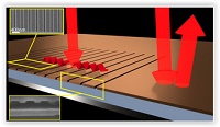
Infra-red devices are used for improved vision through fog and for night vision and for observations not possible with visible light; high-quality detectors cost approximately $100,000 (including the device at the University of Sydney) some require cooling to -200°C.
Now, research spearheaded by researchers at the University of Sydney has demonstrated a dramatic increase in the absorption efficiency of light in a layer of semiconductor that is only a few hundred atoms thick - to almost 99 percent light absorption from the current inefficient 7.7 percent.
The findings will be published overnight in the high-impact journal Optica.
Co-author from the University of Sydney's School of Physics, Professor Martijn de Sterke, said the team discovered perfect thin film light absorbers could be created simply by etching grooves into them.
"Conventional absorbers add bulk and cost to the infrared detector as well as the need for continuous power to keep the temperature down. The ultrathin absorbers can reduce these drawbacks," Professor de Sterke said.
"By etching thin grooves in the film, the light is directed sideways and almost all of it is absorbed, despite the small amount of material - the absorbing layer is less than 1/2000th the thickness of a human hair," he said.
Co-lead author Dr Björn Sturmberg, who carried out the research as a PhD student at the University of Sydney with the support of the Australian Renewable Energy Agency, said the findings did not rely upon a particular material but could be applied to many naturally occurring weak absorbers.
"There are many applications that could greatly benefit from perfectly absorbing ultra-thin films, ranging from defence and autonomous farming robots to medical tools and consumer electronics," Dr Sturmberg said.
The Director of Australia's National Computational Infrastructure (NCI) and co-author, of the paper, Professor Lindsay Botten, said the structures were much simpler to design and fabricate than using existing thin film light absorbers, which required either complex nanostructures, meta-materials and exotic materials or difficult-to-create combinations of metals and non-metals.
"There are major efficiency and sensitivity gains to be obtained from making photo-detectors with less material," he said.
Share on:


Suggested Items
The Big Picture: Our Big ‘Why’ in the Age of AI
06/25/2025 | Mehul Davé -- Column: The Big PictureWith advanced technology, Tesla, Google, Microsoft, and OpenAI can quickly transform life as we know it. Several notable artificial intelligence (AI) studies, including the 2024 McKinsey Global Survey on AI, have offered insights into AI’s adoption, impact, and trajectory. The McKinsey study revealed that AI adoption continues to grow, with 50% of respondents reporting using AI in at least one business area.
Meet Thiago Guimaraes, IPC's New Director of Industry Intelligence
05/05/2025 | Chris Mitchell, IPC VP, Global Government RelationsThe fast pace of innovation in the electronics manufacturing industry means business owners must continuously adapt their processes and capabilities to meet changing customer demands and market trends. To that end, IPC has hired Thiago Guimaraes as the new director of Industry Intelligence. In this interview, Thiago shares key goals and objectives that could revolutionize the industry as he helps stakeholders navigate industry trends and challenges.
Stocks Tumble as Nvidia Warns of Major Hit From U.S.-China Export Curbs
04/17/2025 | I-Connect007 Editorial TeamU.S. stocks slid sharply Wednesday after Nvidia warned that new U.S. export restrictions on chips to China could slash billions from its revenue, deepening investor anxiety over the broader economic fallout of President Donald Trump’s ongoing trade war.
Samsung and Google Cloud Expand Partnership
04/09/2025 | PRNewswireSamsung Electronics Co., Ltd and Google Cloud today announced an expanded partnership to bring Google Cloud's generative AI technology to Ballie, a new home AI companion robot from Samsung.
Insulectro Technology Village to Feature 35 Powerchats at IPC APEX EXPO 2025
03/11/2025 | InsulectroInsulectro, the largest distributor of materials for use in the manufacture of PCBs and printed electronics, will present its popular and successful 13.5-minute PowerChats™ during this year’s IPC APEX EXPO at the Anaheim Convention Center, March 18-20, 2025.