


 Dan’s Biz Bookshelf: Four Important Books You Need to Read (Not Just Say You Have)
 The Marketing Minute: Cracking the Code of Technical Marketing


Tiny Probe Could Produce Big Improvements in Batteries and Fuel Cells
June 1, 2016 | AIP.orgEstimated reading time: 3 minutes
A team of American and Chinese researchers has developed a new tool that could aid in the quest for better batteries and fuel cells.
Although battery technology has come a long way since Alessandro Volta first stacked metal discs in a "voltaic pile" to generate electricity, major improvements are still needed to meet the energy challenges of the future, such as powering electric cars and storing renewable energy cheaply and efficiently.
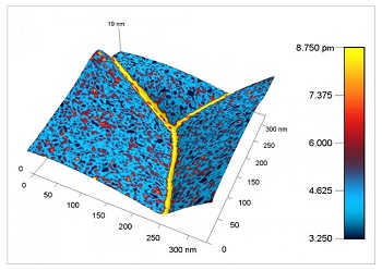
The key to the needed improvements likely lies in the nanoscale, said Jiangyu Li, a professor of Mechanical Engineering at the University of Washington in Seattle. The nanoscale is a realm so tiny that the movement of a few atoms or molecules can shift the landscape. Li and his colleagues have built a new window into this world to help scientists better understand how batteries really work. They describe their nanoscale probe in the Journal of Applied Physics, from AIP Publishing.
Batteries, and their close kin fuel cells, produce electricity through chemical reactions. The rates at which these reactions occur determine how fast the battery can charge, how much power it can provide, and how quickly it degrades.
Although the material in a battery electrode may look uniform to the human eye, to the atoms themselves, the environment is surprisingly diverse.
Near the surface and at the interfaces between materials, huge shifts in properties can occur -- and the shifts can affect the reaction rates in complex and difficult-to-understand ways.
Research in the last ten to fifteen years has revealed just how much local variations in material properties can affect the performance of batteries and other electrochemical systems, Li said.
The complex nanoscale landscape makes it tricky to fully understand what's going on, but "it may also create new opportunities to engineer materials properties so as to achieve quantum leaps in performance," he said.
To get a better understanding of how chemical reactions progress at the level of atoms and molecules, Li and his colleagues developed a nanoscale probe. The method is similar to atomic force microscopies: A tiny cantilever "feels" the material and builds a map of its properties with a resolution of nanometers or smaller.
In the case of the new electrochemical probe, the cantilever is heated with an electrical current, causing fluctuations in temperature and localized stress in the material beneath the probe. As a result, atoms and ions within the material move around, causing it to expand and contract. This expansion and contraction causes the cantilever to vibrate, which can be measured accurately using a laser beam shining on the top of the cantilever.
If a large concentration of ions or other charged particles exist in the vicinity of the probe tip, changes in their concentration will cause the material to deform further, similar to the way wood swells when it gets wet. The deformation is called Vegard strain.
Both Vegard strain and standard thermal expansion affect the vibration of the material, but in different ways. If the vibrations were like musical notes, the thermally-induced Vegard strain is like a harmonic overtone, ringing one octave higher than the note being played, Li explained.
The device identifies the Vegard strain-induced vibrations and can extrapolate the concentration of ions and electronic defects near the probe tip. The approach has advantages over other types of atomic microscopy that use voltage perturbations to generate a response, since voltage can produce many different kinds of responses, and it is difficult to isolate the part of the response related to shifts in ionic and electronic defect concentration. Thermal responses are easier to identify, although one disadvantage of the new system is that it can only probe rates slower than the heat transfer processes in the vicinity of the tip.
Still, the team believes the new method will offer researchers a valuable tool for studying electrochemical material properties at the nanoscale. They tested it by measuring the concentration of charged species in Sm-doped ceria and LiFePO4, important materials in solid oxide fuel cells and lithium batteries, respectively.
"The concentration of ionic and electronic species are often tied to important rate properties of electrochemical materials -- such as surface reactions, interfacial charge transfer, and bulk and surface diffusion -- that govern the device performance," Li said. "By measuring these properties locally on the nanoscale, we can build a much better understanding of how electrochemical systems really work, and thus how to develop new materials with much higher performance."
Share on:


Testimonial
"Advertising in PCB007 Magazine has been a great way to showcase our bare board testers to the right audience. The I-Connect007 team makes the process smooth and professional. We’re proud to be featured in such a trusted publication."
Klaus Koziol - atgSuggested Items
Curing and Verification in PCB Shadow Areas
09/17/2025 | Doug Katze, DymaxDesign engineers know a simple truth that often complicates electronics manufacturing: Light doesn’t go around corners. In densely populated PCBs, adhesives and coatings often fail to fully cure in shadowed regions created by tall ICs, connectors, relays, and tight housings.
Marcy’s Musings: Advancing the Advanced Materials Discussion
09/17/2025 | Marcy LaRont -- Column: Marcy's MusingsAs the industry’s most trusted global source of original content about the electronics supply chain, we continually ask you about your concerns, what you care about, and what you most want to learn about. Your responses are insightful and valuable. Thank you for caring enough to provide useful feedback and engage in dialogue.
September 2025 PCB007 Magazine: The Future of Advanced Materials
09/16/2025 | I-Connect007 Editorial TeamMoore’s Law is no more, and the advanced material solutions being developed to grapple with this reality are surprising, stunning, and perhaps a bit daunting. Buckle up for a dive into advanced materials and a glimpse into the next chapters of electronics manufacturing.
I-Connect007 Launches Advanced Electronics Packaging Digest
09/15/2025 | I-Connect007I-Connect007 is pleased to announce the launch of Advanced Electronics Packaging Digest (AEPD), a new monthly digital newsletter dedicated to one of the most critical and rapidly evolving areas of electronics manufacturing: advanced packaging at the interconnect level.
Panasonic Industry will Double the Production Capacity of MEGTRON Multi-layer Circuit Board Materials Over the Next Five Years
09/15/2025 | Panasonic Industry Co., Ltd.Panasonic Industry Co., Ltd., a Panasonic Group company, announced plans for a major expansion of its global production capacity for MEGTRON multi-layer circuit board materials today. The company plans to double its production over the next five years to meet growing demand in the AI server and ICT infrastructure markets.