


 Dan’s Biz Bookshelf: Four Important Books You Need to Read (Not Just Say You Have)
 The Marketing Minute: Cracking the Code of Technical Marketing


'Weak' Materials Offer Strong Possibilities for Electronics
June 1, 2016 | University of Texas at DallasEstimated reading time: 3 minutes
New fundamental research by UT Dallas physicists may accelerate the drive toward more advanced electronics and more powerful computers.
The scientists are investigating materials called topological insulators, whose surface electrical properties are essentially the opposite of the properties inside.
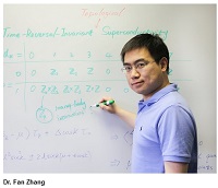
“These materials are made of the same thing throughout, from the interior to the exterior,” said Dr. Fan Zhang, assistant professor of physics at UT Dallas. “But, the interior does not conduct electrons — it’s an insulator — while the electrons on the surface are free to move around. The surface is therefore a conductor, like a metal, but it is in fact more robust than a metal.”
There are two types of topological insulators: strong and weak. The difference between them is subtle and involves complex physics, but is critically important.
“If you had a cube of material that is a strong topological insulator, all six faces can conduct electrons,” Zhang said. “For the weak one, only the four sides are conducting, while the top and bottom surfaces remain insulating.”
Strong topological insulators were made experimentally shortly after they were theoretically proposed. Zhang said they are common in nature, and several dozen variations have been identified and experimentally confirmed.
On the other hand, weak topological insulators have been more elusive. Scientists have proposed various ways to construct a weak topological insulator, but because of its distinctive properties, researchers have not been able to say definitively that they have experimentally produced one.
Zhang, a theoretical physicist, has devised a new way to make a weak topological insulator, one that involves a relatively simple mix of two chemical elements: a crystal composed of bismuth combined with either iodine or bromine. He and his colleagues published the research recently in the journal Physical Review Letters and presented their work at the March meeting of the American Physical Society.
In the 1970s, German scientists grew bismuth iodides and bismuth bromides, but they didn’t understand their potential as weak topological insulators, Zhang said.
“This class of materials we are proposing is a unique platform for exploring exotic physics with fairly simple chemistry,” he said. “With further research and experimentation, our findings could lead to significant advances in technology, especially in electronics and quantum computing.”
Electrically conductive materials are the fundamental building blocks of the traditional transistors that power electronic devices including cellphones and computers. Researchers are developing new theories and experiments with innovative physics and materials to create new transistor-like technologies that run devices and make computers more powerful.
With such exotic electrical properties, topological insulators offer a potential option, Zhang said.
“Our lives have been modified over time by our understanding of the conduction of electrons and the exploitation of this physics for use in electronic devices,” he said. “We now need to revolutionize transistors. One possible substitution is a so-called topological field effect transistor, which could be made of a thin film of a weak topological insulator.”
Computers also are heading for a fundamental redesign, and those efforts might be aided by Zhang’s research.
Page 1 of 2
Share on:


Testimonial
"The I-Connect007 team is outstanding—kind, responsive, and a true marketing partner. Their design team created fresh, eye-catching ads, and their editorial support polished our content to let our brand shine. Thank you all! "
Sweeney Ng - CEE PCBSuggested Items
Curing and Verification in PCB Shadow Areas
09/17/2025 | Doug Katze, DymaxDesign engineers know a simple truth that often complicates electronics manufacturing: Light doesn’t go around corners. In densely populated PCBs, adhesives and coatings often fail to fully cure in shadowed regions created by tall ICs, connectors, relays, and tight housings.
Marcy’s Musings: Advancing the Advanced Materials Discussion
09/17/2025 | Marcy LaRont -- Column: Marcy's MusingsAs the industry’s most trusted global source of original content about the electronics supply chain, we continually ask you about your concerns, what you care about, and what you most want to learn about. Your responses are insightful and valuable. Thank you for caring enough to provide useful feedback and engage in dialogue.
September 2025 PCB007 Magazine: The Future of Advanced Materials
09/16/2025 | I-Connect007 Editorial TeamMoore’s Law is no more, and the advanced material solutions being developed to grapple with this reality are surprising, stunning, and perhaps a bit daunting. Buckle up for a dive into advanced materials and a glimpse into the next chapters of electronics manufacturing.
I-Connect007 Launches Advanced Electronics Packaging Digest
09/15/2025 | I-Connect007I-Connect007 is pleased to announce the launch of Advanced Electronics Packaging Digest (AEPD), a new monthly digital newsletter dedicated to one of the most critical and rapidly evolving areas of electronics manufacturing: advanced packaging at the interconnect level.
Panasonic Industry will Double the Production Capacity of MEGTRON Multi-layer Circuit Board Materials Over the Next Five Years
09/15/2025 | Panasonic Industry Co., Ltd.Panasonic Industry Co., Ltd., a Panasonic Group company, announced plans for a major expansion of its global production capacity for MEGTRON multi-layer circuit board materials today. The company plans to double its production over the next five years to meet growing demand in the AI server and ICT infrastructure markets.