


 Dan’s Biz Bookshelf: Four Important Books You Need to Read (Not Just Say You Have)
 The Marketing Minute: Cracking the Code of Technical Marketing


Tiny Probe Could Produce Big Improvements in Batteries and Fuel Cells
June 1, 2016 | University of WashingtonEstimated reading time: 3 minutes
A team led by University of Washington engineers has developed a new tool that could aid in the quest for better batteries and fuel cells.
Although battery technology has come a long way since Alessandro Volta first stacked metal discs in a “voltaic pile” to generate electricity, major improvements are still needed to meet the energy challenges of the future, such as powering electric cars and storing renewable energy cheaply and efficiently.
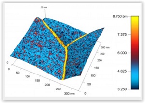
A nanoscale map of the metal ceria produced with a new probe developed by UW engineers shows a higher response, represented by a yellow color, near the boundary between grains of metal. The higher response corresponds to a higher concentration of charged species. Image credit: Ehsan Nasr Esfahani/ University of Washington
The key likely lies in the nanoscale, said Jiangyu Li, UW professor of mechanical engineering. The nanoscale is a realm so tiny that the movement of a few atoms or molecules can shift the landscape. In a paper published May 31 in the Journal of Applied Physics, Li and his colleagues describe a nanoscale probe that offers a new window into this world to help scientists better understand how batteries really work.
Batteries, and their close kin fuel cells, produce electricity through chemical reactions. The rates at which these reactions occur determine how fast the battery can charge, how much power it can provide and how quickly it degrades.
Although the material in a battery electrode may look uniform to the human eye, to the atoms themselves, the environment is surprisingly diverse.
Near the surface and at the interfaces between materials, huge shifts in properties can occur — and the shifts can affect the reaction rates in complex and difficult-to-understand ways.
Research in the last 10 to 15 years has revealed just how much local variations in material properties can affect the performance of batteries and other electrochemical systems, Li said.
The complex nanoscale landscape makes it tricky to fully understand what’s going on, but “it may also create new opportunities to engineer material properties so as to achieve quantum leaps in performance,” he said.
To get a better understanding of how chemical reactions progress at the level of atoms and molecules, Li and his colleagues developed a nanoscale probe. The method is similar to atomic force microscopies: a tiny cantilever “feels” the material and builds a map of its properties with a resolution of nanometers or smaller.
In the case of the new electrochemical probe, the cantilever is heated with an electrical current, causing fluctuations in temperature and localized stress in the material beneath the probe. As a result, atoms and ions within the material move around, causing it to expand and contract. This expansion and contraction causes the cantilever to vibrate, which can be measured accurately using a laser beam shining on the top of the cantilever.
If a large concentration of ions or other charged particles exist in the vicinity of the probe tip, changes in their concentration will cause the material to deform further, similar to the way wood swells when it gets wet. The deformation is called Vegard strain.
Both Vegard strain and standard thermal expansion affect the vibration of the material, but in different ways. If the vibrations were like musical notes, the thermally induced Vegard strain is like a harmonic overtone, ringing one octave higher than the note being played, Li explained.
The device identifies the Vegard strain-induced vibrations and can extrapolate the concentration of ions and electronic defects near the probe tip. The approach has advantages over other types of atomic microscopy that use voltage perturbations to generate a response, since voltage can produce many different kinds of responses, and it is difficult to isolate the part of the response related to shifts in ionic and electronic defect concentration. Thermal responses are easier to identify, although one disadvantage of the new system is that it can only probe rates slower than the heat transfer processes in the vicinity of the tip.
Still, the team believes the new method will offer researchers a valuable tool for studying electrochemical material properties at the nanoscale. They tested it by measuring the concentration of charged species in Sm-doped ceria and LiFePO4, important materials in solid oxide fuel cells and lithium batteries.
“The concentration of ionic and electronic species are often tied to important rate properties of electrochemical materials — such as surface reactions, interfacial charge transfer, and bulk and surface diffusion — that govern the device performance,” Li said. “By measuring these properties locally on the nanoscale, we can build a much better understanding of how electrochemical systems really work, and thus how to develop new materials with much higher performance.”
Share on:


Testimonial
"We’re proud to call I-Connect007 a trusted partner. Their innovative approach and industry insight made our podcast collaboration a success by connecting us with the right audience and delivering real results."
Julia McCaffrey - NCAB GroupSuggested Items
Summit Interconnect Announces Appointment of Leo LaCroix as Chief Operating Officer
09/09/2025 | Summit Interconnect, Inc.Summit Interconnect, a leading North American manufacturer of Printed Circuit Boards (PCBs), today announced that Leo LaCroix has assumed the role of Chief Operating Officer (COO).
UHDI Fundamentals: UHDI Technology and Industry 4.0
09/03/2025 | Anaya Vardya, American Standard CircuitsUltra high density interconnect (UHDI) technology is rapidly transforming how smart systems are designed and deployed in the context of Industry 4.0. With its capacity to support highly miniaturized, high-performance, and densely packed electronics, UHDI is a critical enabler of the smart, connected, and automated industrial future. Here, I’ll explore the synergy between UHDI and Industry 4.0 technologies, highlighting applications, benefits, and future directions.
Mastering PCB Floor Planning
08/28/2025 | Stephen V. Chavez, Siemens EDAPlacement of PCB components is far more than just fitting components onto a board. It’s a strategic and critical foundational step, often called “floor planning,” that profoundly impacts the board’s performance, reliability, manufacturability, and cost. Floor planning ties into the solvability perspective, with performance and manufacturability being the other two competing perspectives for addressing and achieving success in PCB design.
Macronix Introduces Cutting-Edge Secure-Boot NOR Flash Memory
08/08/2025 | PRNewswireMacronix International Co., Ltd., a leading integrated device manufacturer in the non-volatile memory (NVM) market, announced ArmorBoot MX76, a robust NOR flash memory combining in a single device, the essential performance and an array of security features that deliver rapid boot times and iron-clad data protection.
UHDI Fundamentals: UHDI Technology and Industry 4.0
08/05/2025 | Anaya Vardya, American Standard CircuitsUltra high density interconnect (UHDI) technology is rapidly transforming how smart systems are designed and deployed in Industry 4.0. With its capacity to support highly miniaturized, high-performance, and densely packed electronics, UHDI is a critical enabler of the smart, connected, and automated industrial future. This article explores the synergy between UHDI and Industry 4.0 technologies, highlighting applications, benefits, and future directions.