















 It’s Only Common Sense: How AI Consumes the Electronics Supply Chain
 Dan’s Biz Bookshelf: ‘Building a Story Brand 2.0’





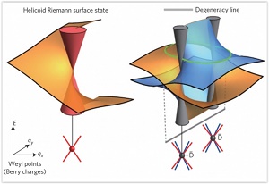
Discovered just five years ago, topological semimetals are materials with unusual physical properties that could make them useful for future electronics.
In the latest issue of Nature Physics, MIT researchers report a new theoretical characterization of topological semimetals’ electrical properties that accurately describes all known topological semimetals and predicts several new ones.
Guided by their model, the researchers also describe the chemical formula and crystal structure of a new topological semimetal that, they reason, should exhibit electrical characteristics never seen before.
“Generally, the properties of a material are sensitive to many external perturbations,” says Liang Fu, an assistant professor of physics at MIT and senior author on the new paper. “What’s special about these topological materials is they have some very robust properties that are insensitive to these perturbations. That’s attractive because it makes theory very powerful in predicting materials, which is rare in condensed-matter physics. Here, we know how to distill or extract the most essential properties, these topological properties, so our methods can be approximate, but our results will be exact.”
Semimetals are somewhat like semiconductors, which are at the core of all modern electronics. Electrons in a semiconductor can be in either the “valence band,” in which they’re attached to particular atoms, or the “conduction band,” in which they’re free to flow through the material as an electrical current. Switching between conductive and nonconductive states is what enables semiconductors to instantiate the logic of binary computation.
Bumping an electron from the valence band into the conduction band requires energy, and the energy differential between the two bands is known as the “band gap.” In a semimetal — such as the much-studied carbon sheets known as graphene — the band gap is zero. In principle, that means that semimetal transistors could switch faster, at lower powers, than semiconductor transistors do.
Parking-garage graphs
The term “topological” is a little more oblique. Topology is a branch of mathematics that treats geometry at a high level of abstraction. Topologically, any object with one hole in it — a coffee cup, a donut, a garden hose — is equivalent to any other. But no amount of deformation can turn a donut into an object with two holes, or none, so two-holed and no-holed objects constitute their own topological classes.
In a topological semimetal, “topological” doesn’t describe the geometry of the material itself; it describes the graph of the relationship between the energy and the momentum of electrons in the material’s surface. Physical perturbations of the material can warp that graph, in the same sense that a donut can be warped into a garden hose, but the material’s electrical properties will remain the same. That’s what Fu means when he says, “Our methods can be approximate, but our results will be exact.”
Fu and his colleagues — joint first authors Chen Fang and Ling Lu, both of whom were MIT postdocs and are now associate professors at the Institute of Physics in Beijing; and Junwei Liu, a postdoc at MIT’s Materials Processing Center — showed that the momentum-energy relationships of electrons in the surface of a topological semimetal can be described using mathematical constructs called Riemann surfaces.
Widely used in the branch of math known as complex analysis, which deals with functions that involve the square root of -1, or i, Riemann surfaces are graphs that tend to look like flat planes twisted into spirals.
“What makes a Riemann surface special is that it’s like a parking-garage graph,” Fu says. “In a parking garage, if you go around in a circle, you end up one floor up or one floor down. This is exactly what happens for the surface states of topological semimetals. If you move around in momentum space, you find that the energy increases, so there’s this winding.”
The researchers showed that a certain class of Riemann surfaces accurately described the momentum-energy relationship in known topological semimetals. But the class also included surfaces that corresponded to electrical characteristics not previously seen in nature.
Page 1 of 2
Share on:



Subscribe
Stay ahead of the technologies shaping the future of electronics with our latest newsletter, Advanced Electronics Packaging Digest. Get expert insights on advanced packaging, materials, and system-level innovation, delivered straight to your inbox.
Subscribe now to stay informed, competitive, and connected.
Suggested Items
Mexico Solders On With Indium Corporation
09/16/2026 | Nolan Johnson, SMT007 MagazineIt makes sense to go where the customers are, which is why Indium Corporation recently opened a new solder paste manufacturing facility in Guadalajara, Mexico. Chris Bastecki, vice president of the Americas Sales and Service Group at Indium Corporation, as well as vice president of PCB Assembly Materials, discusses the reasons behind the new facility, the growing market segments, and the challenges of matching solder to specific applications.
Indium Promotes Chris Bastecki to Business Unit Vice President
09/11/2026 | Indium CorporationIndium Corporation is pleased to announce the promotion of Chris Bastecki to Business Unit Vice President, Americas Sales & Service and Global Printed Circuit Board (PCB) Assembly Materials Marketing.
Indium Promotes Damian Santhanasamy to Global Accounts Manager
09/09/2026 | Indium CorporationWith its commitment to innovation and growth through employee development, Indium Corporation® is pleased to announce the promotion of Damian Santhanasamy to Global Accounts Manager.
Beyond the Chip: Indium Highlights AI Materials Solutions at SEMICON Taiwan 2026
09/04/2026 | Indium CorporationAs artificial intelligence (AI) and high-performance computing (HPC) continue to accelerate semiconductor innovation, the industry is moving beyond the challenge of building a more powerful chip. Increasingly complex packaging, higher power density, tighter thermal requirements, and demands for faster, more cost-effective manufacturing are making system-level performance and the broader manufacturing ecosystem critical to the next generation of AI.
Indium Promotes Hongwen Zhang to Research and Development Director
09/04/2026 | Indium CorporationIndium Corporation has promoted Hongwen Zhang, Ph.D., to Research and Development (R&D) Director. In this role, he will lead technology development, product road-mapping, and the continued advancement of the company’s materials portfolio.