


 Dan’s Biz Bookshelf: Four Important Books You Need to Read (Not Just Say You Have)
 The Marketing Minute: Cracking the Code of Technical Marketing


Glass Now Has Smart Potential
June 8, 2016 | University of AdelaideEstimated reading time: 2 minutes
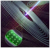
Australian researchers at the University of Adelaide have developed a method for embedding light-emitting nanoparticles into glass without losing any of their unique properties -- a major step towards 'smart glass' applications such as 3D display screens or remote radiation sensors.
This new "hybrid glass" successfully combines the properties of these special luminescent (or light-emitting) nanoparticles with the well-known aspects of glass, such as transparency and the ability to be processed into various shapes including very fine optical fibres.
"These novel luminescent nanoparticles, called upconversion nanoparticles, have become promising candidates for a whole variety of ultra-high tech applications such as biological sensing, biomedical imaging and 3D volumetric displays," says lead author Dr Tim Zhao, from the University of Adelaide's School of Physical Sciences and Institute for Photonics and Advanced Sensing (IPAS).
"Integrating these nanoparticles into glass, which is usually inert, opens up exciting possibilities for new hybrid materials and devices that can take advantage of the properties of nanoparticles in ways we haven't been able to do before. For example, neuroscientists currently use dye injected into the brain and lasers to be able to guide a glass pipette to the site they are interested in. If fluorescent nanoparticles were embedded in the glass pipettes, the unique luminescence of the hybrid glass could act like a torch to guide the pipette directly to the individual neurons of interest."
Although this method was developed with upconversion nanoparticles, the researchers believe their new 'direct-doping' approach can be generalised to other nanoparticles with interesting photonic, electronic and magnetic properties. There will be many applications - depending on the properties of the nanoparticle.
"If we infuse glass with a nanoparticle that is sensitive to radiation and then draw that hybrid glass into a fibre, we could have a remote sensor suitable for nuclear facilities," says Dr Zhao.
To date, the method used to integrate upconversion nanoparticles into glass has relied on the in-situ growth of the nanoparticles within the glass.
"We've seen remarkable progress in this area but the control over the nanoparticles and the glass compositions has been limited, restricting the development of many proposed applications," says project leader Professor Heike Ebendorff-Heideprem, Deputy Director of IPAS.
"With our new direct doping method, which involves synthesizing the nanoparticles and glass separately and then combining them using the right conditions, we've been able to keep the nanoparticles intact and well dispersed throughout the glass. The nanoparticles remain functional and the glass transparency is still very close to its original quality. We are heading towards a whole new world of hybrid glass and devices for light-based technologies."
Share on:


Testimonial
"Advertising in PCB007 Magazine has been a great way to showcase our bare board testers to the right audience. The I-Connect007 team makes the process smooth and professional. We’re proud to be featured in such a trusted publication."
Klaus Koziol - atgSuggested Items
Electra’s ElectraJet EMJ110 Inkjet Soldermask Now in Black & Blue at Sunrise Electronics
09/08/2025 | Electra Polymers LtdFollowing the successful deployment of Electra’s Green EMJ110 Inkjet Soldermask on KLA’s Orbotech Neos™ platform at Sunrise Electronics in Elk Grove Village, Illinois, production has now moved beyond green.
Magnachip Semiconductor Announces YJ Kim to Step Down as CEO; Current Board Chairman Camillo Martino Appointed Interim CEO
08/14/2025 | PR NewswireMagnachip Semiconductor Corporation today announced that YJ Kim has agreed to step down as CEO and as a member of the Board of Directors, effective immediately. Camillo Martino, Chairman of the Board of Directors, has also been appointed Interim Chief Executive Officer, effective immediately.
Bell to Build X-Plane for Phase 2 of DARPA Speed and Runway Independent Technologies (SPRINT) X-Plane Program
07/09/2025 | Bell Textron Inc.Bell Textron Inc., a Textron Inc. company, has been down-selected for Phase 2 of Defense Advanced Research Projects Agency (DARPA) Speed and Runway Independent Technologies (SPRINT) X-Plane program with the objective to complete design, construction, ground testing and certification of an X-plane demonstrator.
Nolan’s Notes: Moving Forward With Confidence
06/03/2025 | Nolan Johnson -- Column: Nolan's NotesWe’re currently enjoying a revitalized and dynamic EMS provider market with significant growth potential. Since December 2024, the book-to-bill has been extremely strong and growing. Starting with a ratio of 1.24 in December, book-to-bill has continued to accelerate to a 1.41 in April. Yet, there is a global economic restructuring taking place. To say that the back-and-forth with tariffs and trade deals makes for an uncertain market is an understatement. While we may be in a 90-day tariff pause among leading economic nations, the deadline is quickly approaching and that leaves many of you feeling unsettled about what to expect.
Mycronic High Flex Changes Division Name to PCB Assembly Solutions
05/20/2025 | MycronicMycronic AB, the leading Sweden-based electronics assembly solutions provider, announced that its division formerly known as High Flex will now operate under the name PCB Assembly Solutions.