


 Dan’s Biz Bookshelf: Four Important Books You Need to Read (Not Just Say You Have)
 The Marketing Minute: Cracking the Code of Technical Marketing


Spintronics Development Gets Boost with New Findings into Ferromagnetism in Mn-doped GaAs
June 9, 2016 | Tohoku UniversityEstimated reading time: 2 minutes
A research group at Tohoku University's WPI-AIMR has succeeded in finding the origin and the mechanism of ferromagnetism in Mn-doped GaAs. The discovery is significant as it will accelerate the development of the spintronic element.
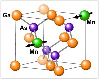
Fig.1: Crystal structure of (Ga,Mn)As. Mn ions substituted for Ga have a magnetic moment, and the magnetic moment of each Mn ion aligns along the same direction when (Ga,Mn)As becomes a ferromagnet.
GaAs, like silicon, is a well-known semiconductor commonly used in high-speed electronic devices and laser diodes.
When manganese (Mn) atoms are doped into a GaAs crystal ((Ga,Mn)As), the crystal exhibits characteristics and properties of both the semiconductor and magnet (Fig. 1). Since it is possible to use an electric field to control the magnetism in (Ga,Mn)As, Mn-doped GaAs has been a key material in spintronic devices and a significant contributor to the development of spintronics technology.
However, although it has been 20 years since that discovery, the mechanism of ferromagnetism in (Ga,Mn)As is still not widely understood or well explained. There remains fierce debate and confusion, leading to obstacles preventing the progress and further development of spintronics technology.
The researchers at Tohoku University, led by Profs. H. Ohno and T. Takahashi, have succeeded in directly observing the electronic states which participate in creating the ferromagnetism by photoemission spectroscopy. They found that doped Mn atoms extract electrons from As atoms, leaving "holes" (empty states of electrons) in the As orbital. This then causes the ferromagnetism in (Ga,Mn)As (seen in Fig. 2).
Fig.2: Two conflicting mechanisms to explain the origin of magnetism in (Ga,Mn)As. The p-d Zener model (a) explains that the ferromagnetism of (Ga,Mn)As is mediated by hole carriers generated in the As-bonding state. On the other hand, the impurity model (b) assumes a different hole character in the newly formed Mn-impurity state located above the As-bonding state. The present study has revealed that the p-d Zener model is a correct description to explain the ferromagnetism of (Ga,Mn)As.
"This finding resolves the long-standing problem in the mechanism of ferromagnetism in (Ga,Mn)As," says researcher Seigo Souma. "It also accelerates the materials engineering of magnetic semiconductors, as well as the tunable controlling of spin states in spintronic devices. This is very significant result and we're excited about the potential it represents."
About AIMR
The Advanced Institute for Materials Research (AIMR) at Tohoku University is one of nine World Premier International Research Center Initiative (WPI) Programs established with the support of the Japanese government. It aims to develop world-class research bases in Japan. Since its establishment in 2007, AIMR has been active in conducting research activities and creating new systems in order to become a global center for materials science. In recent years, AIMR has also been conducting fundamental research by finding connections between materials science and mathematics.
Share on:


Testimonial
"The I-Connect007 team is outstanding—kind, responsive, and a true marketing partner. Their design team created fresh, eye-catching ads, and their editorial support polished our content to let our brand shine. Thank you all! "
Sweeney Ng - CEE PCBSuggested Items
Curing and Verification in PCB Shadow Areas
09/17/2025 | Doug Katze, DymaxDesign engineers know a simple truth that often complicates electronics manufacturing: Light doesn’t go around corners. In densely populated PCBs, adhesives and coatings often fail to fully cure in shadowed regions created by tall ICs, connectors, relays, and tight housings.
Marcy’s Musings: Advancing the Advanced Materials Discussion
09/17/2025 | Marcy LaRont -- Column: Marcy's MusingsAs the industry’s most trusted global source of original content about the electronics supply chain, we continually ask you about your concerns, what you care about, and what you most want to learn about. Your responses are insightful and valuable. Thank you for caring enough to provide useful feedback and engage in dialogue.
September 2025 PCB007 Magazine: The Future of Advanced Materials
09/16/2025 | I-Connect007 Editorial TeamMoore’s Law is no more, and the advanced material solutions being developed to grapple with this reality are surprising, stunning, and perhaps a bit daunting. Buckle up for a dive into advanced materials and a glimpse into the next chapters of electronics manufacturing.
I-Connect007 Launches Advanced Electronics Packaging Digest
09/15/2025 | I-Connect007I-Connect007 is pleased to announce the launch of Advanced Electronics Packaging Digest (AEPD), a new monthly digital newsletter dedicated to one of the most critical and rapidly evolving areas of electronics manufacturing: advanced packaging at the interconnect level.
Panasonic Industry will Double the Production Capacity of MEGTRON Multi-layer Circuit Board Materials Over the Next Five Years
09/15/2025 | Panasonic Industry Co., Ltd.Panasonic Industry Co., Ltd., a Panasonic Group company, announced plans for a major expansion of its global production capacity for MEGTRON multi-layer circuit board materials today. The company plans to double its production over the next five years to meet growing demand in the AI server and ICT infrastructure markets.