


 It’s Only Common Sense: Creativity Is Noisy, Messy, and So Worth It
 Dan’s Biz Bookshelf: ‘The Soul of a New Machine’


Hotel managers and materials scientists have a lot in common — they both need to find a way to control properties by managing vacancies.
Researchers at the U.S. Department of Energy's (DOE's) Argonne National Laboratory found they could use a small electric current to introduce oxygen voids, or vacancies, that dramatically change the conductivity of thin oxide films. The results are published in Nature Communications.
The discovery improves our understanding of how these materials work and could be useful for new electronics, catalysts or more.
Scientists are always looking for unusual behaviors in materials that could form the basis of new technologies. Oxides are a class of materials that has garnered much recent interest because they sometimes display such unusual behaviors — flipping between insulating and conducting states, turning magnetism on and off or even becoming superconducting: conducting electricity perfectly, without any loss as heat.
We think some of these properties have to do with oxygen vacancies. The structure of an oxide is a repeating crystalline lattice with oxygen atoms peppered throughout, but sometimes there may be voids where an oxygen atom is missing.
The usual way to create oxygen vacancies is by heating the materials and adding or removing oxygen from the environment.
"But the need to control the gas environment limits where and when you can change the material's properties," said Jeff Eastman, an Argonne materials scientist and corresponding author on the paper.
The Argonne team wanted to find out if they could control vacancies with an alternate method.
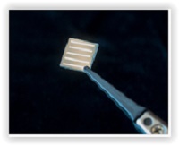
They built a two-layer material: an indium oxide crystal layer on top of a block of yttria-stabilized zirconia. When the researchers applied a small electric field, they watched the electrical conductivity skyrocket by two orders of magnitude along the boundary where the two layers meet. The effect is reversible; without the field, it reverts back to the initial, less conductive state.
"You could imagine applications for electronics or building catalysts — for example, providing a way to split water or carbon dioxide," Eastman said.
The theory, assisted by computational modeling, is that the difference between the properties of the two materials creates a vertical voltage between them, and negatively charged oxygen ions in the indium oxide are attracted to the flow and move across the interface — leaving vacancies behind.
The team is planning further investigation into whether the same effects occur in other materials and whether the method could control other properties, Eastman said.
The co-authors on the paper, "Interfacial Control of Oxygen Vacancy Doping and Electrical Conduction in Thin Film Oxide Heterostructures," are Argonne scientists Boyd Veal, Peter Zapol, Hakim Iddir, and Peter Baldo, and Seong Keun Kim, an Argonne postdoctoral researcher during this study, now a research scientist at the Korea Institute of Science and Technology.
The team used beamline 12-ID at the Advanced Photon Source, a DOE Office of Science User Facility, for characterization and analysis. They also used the Fusion cluster at the Argonne Laboratory Computing Resource Center in evaluating the theory developed.
The research was supported by the DOE Office of Science, Office of Basic Energy Sciences.


