


 Dan’s Biz Bookshelf: Four Important Books You Need to Read (Not Just Say You Have)
 The Marketing Minute: Cracking the Code of Technical Marketing


New Nanomaterial Offers Promise in Bendable, Wearable Electronic Devices
June 13, 2016 | University of Illinois at ChicagoEstimated reading time: 2 minutes
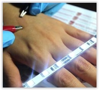
An ultrathin film that is both transparent and highly conductive to electric current has been produced by a cheap and simple method devised by an international team of nanomaterials researchers from the University of Illinois at Chicago and Korea University.
The film -- actually a mat of tangled nanofiber, electroplated to form a "self-junctioned copper nano-chicken wire" -- is also bendable and stretchable, offering potential applications in roll-up touchscreen displays, wearable electronics, flexible solar cells and electronic skin.
The finding is reported in the June 13 issue of Advanced Materials.
"It's important, but difficult, to make materials that are both transparent and conductive," says Alexander Yarin, UIC Distinguished Professor of Mechanical Engineering, one of two corresponding authors on the publication.
The new film establishes a "world-record combination of high transparency and low electrical resistance," the latter at least 10-fold greater than the previous existing record, said Sam Yoon, who is also a corresponding author and a professor of mechanical engineering at Korea University.
The film also retains its properties after repeated cycles of severe stretching or bending, Yarin said -- an important property for touchscreens or wearables.
Manufacture begins by electrospinning a nanofiber mat of polyacrylonitrile, or PAN, whose fibers are about one-hundredth the diameter of a human hair. The fiber shoots out like a rapidly coiling noodle, which when deposited onto a surface intersects itself a million times, Yarin said.
"The nanofiber spins out in a spiral cone, but forms fractal loops in flight," Yarin said. "The loops have loops, so it gets very long and very thin."
The naked PAN polymer doesn't conduct, so it must first be spatter-coated with a metal to attract metal ions. The fiber is then electroplated with copper -- or silver, nickel or gold.
The electrospinning and electroplating are both relatively high-throughput, commercially viable processes that take only a few seconds each, according to the researchers.
"We can then take the metal-plated fibers and transfer to any surface -- the skin of the hand, a leaf, or glass," Yarin said. An additional application may be as a nano-textured surface that dramatically increases cooling efficiency.
Yoon said the "self-fusion" by electroplating at the fiber junctions "dramatically reduced the contact resistance." Yarin noted that the metal-plated junctions facilitated percolation of the electric current -- and also account for the nanomaterial's physical resiliency.
"But most of it is holes," he said, which makes it 92 percent transparent. "You don't see it."
Share on:


Testimonial
"Our marketing partnership with I-Connect007 is already delivering. Just a day after our press release went live, we received a direct inquiry about our updated products!"
Rachael Temple - AlltematedSuggested Items
Electrodeposited Copper Foils Market to Grow by $11.7 Billion Over 2025-2032
09/18/2025 | Globe NewswireThe global electrodeposited copper foils market is poised for dynamic growth, driven by the rising adoption in advanced electronics and renewable energy storage solutions.
MacDermid Alpha Showcases Advanced Interconnect Solutions at PCIM Asia 2025
09/18/2025 | MacDermid Alpha Electronics SolutionsMacDermid Alpha Electronic Solutions, a global leader in materials for power electronics and semiconductor assembly, will showcase its latest interconnect innovations in electronic interconnect materials at PCIM Asia 2025, held from September 24 to 26 at the Shanghai New International Expo Centre, Booth N5-E30
Trouble in Your Tank: Implementing Direct Metallization in Advanced Substrate Packaging
09/15/2025 | Michael Carano -- Column: Trouble in Your TankDirect metallization systems based on conductive graphite are gaining popularity throughout the world. The environmental and productivity gains achievable with this process are outstanding. Direct metallization reduces the costs of compliance, waste treatment, and legal issues related to chemical exposure. A graphite-based direct plate system has been devised to address these needs.
Closing the Loop on PCB Etching Waste
09/09/2025 | Shawn Stone, IECAs the PCB industry continues its push toward greener, more cost-efficient operations, Sigma Engineering’s Mecer System offers a comprehensive solution to two of the industry’s most persistent pain points: etchant consumption and rinse water waste. Designed as a modular, fully automated platform, the Mecer System regenerates spent copper etchants—both alkaline and acidic—and simultaneously recycles rinse water, transforming a traditionally linear chemical process into a closed-loop system.
Driving Innovation: Depth Routing Processes—Achieving Unparalleled Precision in Complex PCBs
09/08/2025 | Kurt Palmer -- Column: Driving InnovationIn PCB manufacturing, the demand for increasingly complex and miniaturized designs continually pushes the boundaries of traditional fabrication methods, including depth routing. Success in these applications demands not only on robust machinery but also sophisticated control functions. PCB manufacturers rely on advanced machine features and process methodologies to meet their precise depth routing goals. Here, I’ll explore some crucial functions that empower manufacturers to master complex depth routing challenges.