


 Dan’s Biz Bookshelf: Four Important Books You Need to Read (Not Just Say You Have)
 The Marketing Minute: Cracking the Code of Technical Marketing


Shaping Atomically Thin Materials in Suspended Structures
June 14, 2016 | Tohoku UniversityEstimated reading time: 1 minute
Researchers at Tohoku University have realized wafer-scale and high yield synthesis of suspended graphene nanoribbons. The unique growth dynamic has been elucidated through comparing experiments, molecular dynamics simulations and theoretical calculations made with researchers from the University of Tokyo and Hokkaido University.
Adding a mechanical degree of freedom to the electrical and optical properties of atomically thin materials can provide an excellent platform to investigate various optoelectrical physics and devices with mechanical motion interaction. The large scale fabrication of such atomically thin materials with suspended structures, remains a challenge.
Led by Associate Prof. Toshiaki Kato, the team has used a bottom-up approach to demonstrate wafer-scale, high-yield synthesis of suspended graphene nanoribbon. This method has shed light on growth dynamics. It is possible to integrate over 1,000,000 suspended graphene nanoribbons in wafer-scale substrate with a high yield of over 90 %.
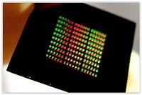
Suspended graphene nanoribbons in wafer-scale.
"Shaping atomically thin materials in suspended structures may provide a viable platform for nanoscale mechanical oscillators," says Kato.
Graphene nanoribbons are strips of graphene with quasi 1D structure (width ∼ a few tens nm, length, ∼ few µm). Different from 2D graphene, graphene nanoribbon includes band gap depending on its width and edge structures. It is expected to be utilized in next generation high performance optoelectrical semiconductor applications.
Kato adds, "The actualization of high yield and wafer-scale synthesis of suspended graphene nanoribbon will have an impact on the study of graphene nanoribbon, and be used in practical applications in a wide variety of fields."
Share on:


Testimonial
"In a year when every marketing dollar mattered, I chose to keep I-Connect007 in our 2025 plan. Their commitment to high-quality, insightful content aligns with Koh Young’s values and helps readers navigate a changing industry. "
Brent Fischthal - Koh YoungSuggested Items
Curing and Verification in PCB Shadow Areas
09/17/2025 | Doug Katze, DymaxDesign engineers know a simple truth that often complicates electronics manufacturing: Light doesn’t go around corners. In densely populated PCBs, adhesives and coatings often fail to fully cure in shadowed regions created by tall ICs, connectors, relays, and tight housings.
Marcy’s Musings: Advancing the Advanced Materials Discussion
09/17/2025 | Marcy LaRont -- Column: Marcy's MusingsAs the industry’s most trusted global source of original content about the electronics supply chain, we continually ask you about your concerns, what you care about, and what you most want to learn about. Your responses are insightful and valuable. Thank you for caring enough to provide useful feedback and engage in dialogue.
September 2025 PCB007 Magazine: The Future of Advanced Materials
09/16/2025 | I-Connect007 Editorial TeamMoore’s Law is no more, and the advanced material solutions being developed to grapple with this reality are surprising, stunning, and perhaps a bit daunting. Buckle up for a dive into advanced materials and a glimpse into the next chapters of electronics manufacturing.
I-Connect007 Launches Advanced Electronics Packaging Digest
09/15/2025 | I-Connect007I-Connect007 is pleased to announce the launch of Advanced Electronics Packaging Digest (AEPD), a new monthly digital newsletter dedicated to one of the most critical and rapidly evolving areas of electronics manufacturing: advanced packaging at the interconnect level.
Panasonic Industry will Double the Production Capacity of MEGTRON Multi-layer Circuit Board Materials Over the Next Five Years
09/15/2025 | Panasonic Industry Co., Ltd.Panasonic Industry Co., Ltd., a Panasonic Group company, announced plans for a major expansion of its global production capacity for MEGTRON multi-layer circuit board materials today. The company plans to double its production over the next five years to meet growing demand in the AI server and ICT infrastructure markets.