


 Dan’s Biz Bookshelf: Four Important Books You Need to Read (Not Just Say You Have)
 The Marketing Minute: Cracking the Code of Technical Marketing


A Light Microscope Made Only with Consumer Electronic Products
June 14, 2016 | ICFOEstimated reading time: 3 minutes
Light microscopes based on scattering, reflection and absorption, or a combination of these, have been a key enabling technology for the study of objects invisible to our eyes, especially in the field of biology. Many improvements have been made in the past to create state-of-the-art techniques capable of achieving unprecedented resolution and sensitivity albeit their cost, which drastically increases with quality and versatility, making them quite unavailable for general applications.
Holographic, phase contrast or differential interference contrast (DIC) miscroscopes have been implemented especially for making "visible", otherwise "invisible", transparent objects, opening a new pathway towards the study and characterization of relevant structures such as biological cells or protein layers. The DIC microscope invented by Carl Zeiss several decades ago is one of the most popular in this field.
Now, even though these techniques have offered high sensitivity and resolution, they have shown to be severely limited as far as field-of-view (FOV) and depth-of-field (DOF), a major drawback and great limitation when it comes to large samples, where a scanning method is mandatory and time consuming. The trade-off will always be there: when trying to improve one parameter with a specific combination of lenses, the other will deteriorate.
Therefore, in recent years, research has been focused on developing microscopes without optical lenses or objectives that could offer unprecedented FOV while maintaining fair sensitivity and resolution.
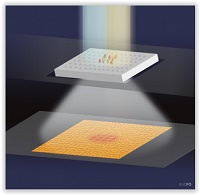
In a paper published in Science Advances, ICFO researchers Roland Terborg, Josselin Pello, Ilaria Mannelli, UPC Prof. at ICFO Juan P. Torres and ICREA Prof. at ICFO Valerio Pruneri, have built a novel low-cost, compact on-chip microscope, made with consumer electronic products, capable of simultaneously measuring nanometer-thick changes over a large volume (0.5cm^3) in transparent objects such as glass.
The researchers have developed a large FOV interferometric on-chip lens free microscope (LIM) based on a novel design with a very high axial sensitivity and DOF, applying a technique adequate to be used in microarray platforms for the detection of proteins without the need of labels.
As Roland Terborg comments, "The challenge of developing a lens-free microscope to detect single protein layers (less than 1nm of optical path difference) seemed rather difficult at the beginning. But as we started to develop the device, everything seemed to fit in very well surpassing our expectations! Instead of having to use very expensive components, we discovered that we could actually use consumer end products without a significant decrease in its sensitivity".
By using collimated polarized light, the team of scientists was able to reconstruct the image by shining light through the transparent sample to observe and analyze the phase shift and interference intensity pattern, a technique known as phase-shifting interferometry (PSI). As UPC Prof at ICFO Juan P. Torres states, "any slight refractive index change introduced by an impurity in the sample is translated into a phase difference and thus an intensity variation in the pattern, showing the contours and therefore size of the irregularity".
As ICREA Prof. at ICFO Valerio Pruneri comments "the device means a major step forward for light microscopy techniques, especially for microarray platforms since it could definitely be used as a point-of-care tool in the diagnosis and treatment of major diseases such as Sepsis, a critical area where fast and accurate results can translate into life changing health outcomes for individuals. We are also thrilled by the fact that this will be part of the Sixsenso spin-off project portfolio including similar devices for detection of particulates and micro-organisms".
The new device has proven to be low-cost, compact, and extremely suitable for point-of-care applications, making it an ideal device to be fully integrated in cameras of smart phones or tablets and used for detecting and scanning of transparent objects or surfaces.
Share on:


Testimonial
"We’re proud to call I-Connect007 a trusted partner. Their innovative approach and industry insight made our podcast collaboration a success by connecting us with the right audience and delivering real results."
Julia McCaffrey - NCAB GroupSuggested Items
Electra’s ElectraJet EMJ110 Inkjet Soldermask Now in Black & Blue at Sunrise Electronics
09/08/2025 | Electra Polymers LtdFollowing the successful deployment of Electra’s Green EMJ110 Inkjet Soldermask on KLA’s Orbotech Neos™ platform at Sunrise Electronics in Elk Grove Village, Illinois, production has now moved beyond green.
Magnachip Semiconductor Announces YJ Kim to Step Down as CEO; Current Board Chairman Camillo Martino Appointed Interim CEO
08/14/2025 | PR NewswireMagnachip Semiconductor Corporation today announced that YJ Kim has agreed to step down as CEO and as a member of the Board of Directors, effective immediately. Camillo Martino, Chairman of the Board of Directors, has also been appointed Interim Chief Executive Officer, effective immediately.
Bell to Build X-Plane for Phase 2 of DARPA Speed and Runway Independent Technologies (SPRINT) X-Plane Program
07/09/2025 | Bell Textron Inc.Bell Textron Inc., a Textron Inc. company, has been down-selected for Phase 2 of Defense Advanced Research Projects Agency (DARPA) Speed and Runway Independent Technologies (SPRINT) X-Plane program with the objective to complete design, construction, ground testing and certification of an X-plane demonstrator.
Nolan’s Notes: Moving Forward With Confidence
06/03/2025 | Nolan Johnson -- Column: Nolan's NotesWe’re currently enjoying a revitalized and dynamic EMS provider market with significant growth potential. Since December 2024, the book-to-bill has been extremely strong and growing. Starting with a ratio of 1.24 in December, book-to-bill has continued to accelerate to a 1.41 in April. Yet, there is a global economic restructuring taking place. To say that the back-and-forth with tariffs and trade deals makes for an uncertain market is an understatement. While we may be in a 90-day tariff pause among leading economic nations, the deadline is quickly approaching and that leaves many of you feeling unsettled about what to expect.
Mycronic High Flex Changes Division Name to PCB Assembly Solutions
05/20/2025 | MycronicMycronic AB, the leading Sweden-based electronics assembly solutions provider, announced that its division formerly known as High Flex will now operate under the name PCB Assembly Solutions.