


 Dan’s Biz Bookshelf: Four Important Books You Need to Read (Not Just Say You Have)
 The Marketing Minute: Cracking the Code of Technical Marketing


A New Form of Hybrid Photodetectors with Quantum Dots and Graphene
June 20, 2016 | ICFOEstimated reading time: 2 minutes
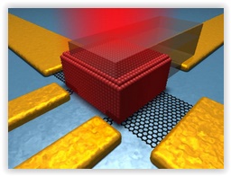
The development of photodetectors has been a matter of considerable interest in the past decades since their applications are essential to many different fields including cameras, medical devices, safety equipment, optical communication devices or even surveying instruments, among others.
Many efforts have been focused towards optoelectronic research in trying to create low cost photodetectors with high sensitivity, high quantum efficiency, high gain and fast photoresponse. This is of paramount importance especially in the short wave infrared which currently is addressed by very expensive III-V InGaAs photodetectors. The development of two main classes of photodetectors, photodiodes and phototransistors, have partially been able to accomplish these goals because even though they both have many outstanding properties, none seem to fulfill all of these requirements. While photodiodes are much faster than phototransistors, phototransistors have a higher gain and do not require low noise preamplifiers for their use.
To overcome these limitations, ICFO researchers Ivan Nikitskiy, Stijn Goossens, Dominik Kufer, Tania Lasanta, Gabriele Navickaite, led by ICREA professors at ICFO Frank Koppens and Gerasimos Konstantatos, have been able to develop a hybrid photodetector capable of attaining concomitantly better performance features in terms of speed, quantum efficiency and linear dynamic range, operating not only in the visible but also in the near infrared (NIR: 700-1400nm) and SWIR range (1400-3000nm). At the same time this technology is based upon materials that can be monolithically integrated with Si CMOS electronics as well as flexible electronic platforms. The results of this work have been recently published in Nature Communications.
To be able to achieve this, the team of researchers developed a hybrid device by integrating an active colloidal quantum dot photodiode with a graphene phototransistor. By including an "active" quantum dot photodiode, they were able to increase charge collection in a highly absorbing thick QD film, which in turn increased the quantum efficiency as well as the photoresponse. The active quantum dot layer enabled a more effective charge collection by exploiting carrier drift towards the graphene layer instead of relying only on diffusion. The researchers then combined this scheme with a graphene transistor to register ultra-high-gains and record gain-bandwidth products, thanks to Graphene's 2D character and remarkably high carrier mobility.
The results obtained in this study have shown that this hybrid architecture does clearly demonstrate the potential of graphene and active quantum dot materials, opening new pathways for their integration in other optoelectronic materials in search for much higher performance and a broader spectrum of functionalities.
Share on:


Testimonial
"In a year when every marketing dollar mattered, I chose to keep I-Connect007 in our 2025 plan. Their commitment to high-quality, insightful content aligns with Koh Young’s values and helps readers navigate a changing industry. "
Brent Fischthal - Koh YoungSuggested Items
Curing and Verification in PCB Shadow Areas
09/17/2025 | Doug Katze, DymaxDesign engineers know a simple truth that often complicates electronics manufacturing: Light doesn’t go around corners. In densely populated PCBs, adhesives and coatings often fail to fully cure in shadowed regions created by tall ICs, connectors, relays, and tight housings.
Marcy’s Musings: Advancing the Advanced Materials Discussion
09/17/2025 | Marcy LaRont -- Column: Marcy's MusingsAs the industry’s most trusted global source of original content about the electronics supply chain, we continually ask you about your concerns, what you care about, and what you most want to learn about. Your responses are insightful and valuable. Thank you for caring enough to provide useful feedback and engage in dialogue.
September 2025 PCB007 Magazine: The Future of Advanced Materials
09/16/2025 | I-Connect007 Editorial TeamMoore’s Law is no more, and the advanced material solutions being developed to grapple with this reality are surprising, stunning, and perhaps a bit daunting. Buckle up for a dive into advanced materials and a glimpse into the next chapters of electronics manufacturing.
I-Connect007 Launches Advanced Electronics Packaging Digest
09/15/2025 | I-Connect007I-Connect007 is pleased to announce the launch of Advanced Electronics Packaging Digest (AEPD), a new monthly digital newsletter dedicated to one of the most critical and rapidly evolving areas of electronics manufacturing: advanced packaging at the interconnect level.
Panasonic Industry will Double the Production Capacity of MEGTRON Multi-layer Circuit Board Materials Over the Next Five Years
09/15/2025 | Panasonic Industry Co., Ltd.Panasonic Industry Co., Ltd., a Panasonic Group company, announced plans for a major expansion of its global production capacity for MEGTRON multi-layer circuit board materials today. The company plans to double its production over the next five years to meet growing demand in the AI server and ICT infrastructure markets.