


 Dan’s Biz Bookshelf: Four Important Books You Need to Read (Not Just Say You Have)
 The Marketing Minute: Cracking the Code of Technical Marketing


Gate-All-Around MOSFETs with Lateral Silicon Nanowires at Scaled Dimensions
June 20, 2016 | ImecEstimated reading time: 2 minutes
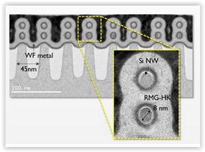
At the 2016 Symposia on VLSI Technology & Circuits, nano-electronics research center imec presented gate-all-around (GAA) n- and p-MOSFET devices made of vertically stacked horizontal silicon (Si) nanowires (NWs) with a diameter of only 8-nm. The devices, which were fabricated on bulk Si substrates using an industry-relevant replacement metal gate (RMG) process, have excellent short-channel characteristics (SS = 65 mV/dec, DIBL = 42 mV/V for LG = 24 nm) at performance levels comparable to finFET reference devices.
GAA devices architectures offer optimal electrostatic control, thereby enabling ultimate CMOS device scaling. In addition, horizontal NWs are a natural extension of RMG finFETs, in contrast to vertical NWs which require more disruptive technology changes. Furthermore, stacking of NWs maximizes the drive current per footprint. Imec successfully combined these three aspects, and, for the first time, demonstrated vertically stacked horizontal Si NWs at scaled dimensions: 8-nm-diameter wires, 45-nm lateral pitch, and 20-nm vertical separation.
Compared to the conventional bulk FinFET flow, imec implemented two major differences in the process flow. First, shallow trench isolation (STI) densification at 750°C resulted to preserve sharp silicon-germanium (SiGe)/Si interfaces, which is essential for well-controlled Si NW release. Second, a low-complexity ground plane doping scheme was applied, suppressing the bottom parasitic channel.
“By demonstrating stacked nanowires with solid electrostatic control, at scaled dimensions, and using an industry-relevant RMG process on bulk silicon substrates, imec has achieved breakthrough results that can pave the way to realizing sub-10nm technology nodes,” stated Dan Mocuta, Director Logic Device and Integration at imec. “The upcoming research phase will focus on achieving even denser pitches and on leveraging this knowledge to develop gate-all-around lateral nanowire CMOS devices.”
Imec’s research into advanced logic scaling is performed in cooperation with imec’s key partners in its core CMOS programs including GlobalFoundries, Intel, Micron, SK Hynix, Samsung, TSMC, Huawei, Qualcomm and Sony.
About imec
Imec performs world-leading research in nanoelectronics and photovoltaics. Imec leverages its scientific knowledge with the innovative power of its global partnerships in ICT, healthcare and energy. Imec delivers industry-relevant technology solutions. In a unique high-tech environment, its international top talent is committed to providing the building blocks for a better life in a sustainable society. Imec is headquartered in Leuven, Belgium, and has offices in Belgium, the Netherlands, Taiwan, USA, China, India and Japan. Its staff of about 2,500 people includes about 740 industrial residents and guest researchers. In 2015, imec's revenue (P&L) totaled 415 million euro.
Share on:


Testimonial
"In a year when every marketing dollar mattered, I chose to keep I-Connect007 in our 2025 plan. Their commitment to high-quality, insightful content aligns with Koh Young’s values and helps readers navigate a changing industry. "
Brent Fischthal - Koh YoungSuggested Items
Technica USA Advocates for PCBAA Membership Among Printed Circuit Assembly Customers
09/16/2025 | Technica USATechnica USA is actively encouraging its printed circuit assembly customers to join the Printed Circuit Board Association of America (PCBAA), a leading industry organization advocating for increased domestic production of printed circuit boards (PCBs) and substrates.
Marcy’s Musings: Advancing the Advanced Materials Discussion
09/17/2025 | Marcy LaRont -- Column: Marcy's MusingsAs the industry’s most trusted global source of original content about the electronics supply chain, we continually ask you about your concerns, what you care about, and what you most want to learn about. Your responses are insightful and valuable. Thank you for caring enough to provide useful feedback and engage in dialogue.
I-Connect007 Launches Advanced Electronics Packaging Digest
09/15/2025 | I-Connect007I-Connect007 is pleased to announce the launch of Advanced Electronics Packaging Digest (AEPD), a new monthly digital newsletter dedicated to one of the most critical and rapidly evolving areas of electronics manufacturing: advanced packaging at the interconnect level.
ICAPE Group Unveils Exclusive Report on Sustainability in Electronics Manufacturing
09/15/2025 | ICAPE GroupICAPE Group, a global leader in printed circuit boards (PCBs) and custom electronics manufacturing, today announces the launch of its 2025 Industry Outlook & Innovation Report: Sustainability in Electronics Manufacturing. This exclusive report is accompanied by fresh insights from a dedicated Statista survey of 100 electronics manufacturing professionals, commissioned by ICAPE Group.
Panasonic Industry will Double the Production Capacity of MEGTRON Multi-layer Circuit Board Materials Over the Next Five Years
09/15/2025 | Panasonic Industry Co., Ltd.Panasonic Industry Co., Ltd., a Panasonic Group company, announced plans for a major expansion of its global production capacity for MEGTRON multi-layer circuit board materials today. The company plans to double its production over the next five years to meet growing demand in the AI server and ICT infrastructure markets.