


 Dan’s Biz Bookshelf: Four Important Books You Need to Read (Not Just Say You Have)
 The Marketing Minute: Cracking the Code of Technical Marketing


Coexistence of Superconductivity and Charge Density Waves Observed
June 22, 2016 | IRIS AdlershofEstimated reading time: 1 minute
Physicists at BESSY II studied an artificial structure composed of alternating layers of ferromagnetic and superconducting materials. Charge density waves induced by the interfaces were found to extend deeply into the superconducting regions, indicating new ways to manipulate superconductivity. The results are now being published in Nature Materials.
High-Tc superconductors were discovered 30 years ago: A class of ceramic metal oxide materials was found to pass electrical current without energy losses. In contrast to conventional superconductors that have to be cooled almost to absolute zero, this property appears already at comparably high temperatures. In prototypical yttrium barium copper oxide (YBaCuO), the transition temperature is 92 Kelvin (minus 181 degrees centigrade). Hence, liquid nitrogen suffices as coolant to reach the superconducting phase. The discovery of high-temperature superconductivity has started a quest for applications, which are being implemented now. Until now, however, the microscopic mechanism of high-Tc superconductivity is still matter of debate.
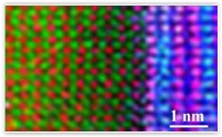
Superconducting and feromagnetic thin layers
A team of scientists lead by Prof. Bernhard Keimer, MPI for Solid State Research, and Dr. Eugen Weschke, HZB, have now investigated an artificial layer system composed of alternating nanolayers of YBaCuO and a ferromagnetic material. The thicknesses of the YBaCuO layers varied between 10 nm and 50 nm.
Tiny collective modulations of valence electrons observed
As interfaces often determine the properties of such heterostructures, physicists were particularly interested in their role for the present system. During his PhD work using resonant x-ray diffraction at BESSY II, Alex Frano could detect tiny collective modulations of valence electrons around Cu atoms in the YBaCuO layer. Data analysis revealed that the resulting charge density wave does not remain located close to the interface but extends across the whole layer. “ This finding is quite a surprise, as previous studies revealed a strong tendency of superconductivity to suppress the formation of charge density waves”, explains Frano.
Charge density wave is stabilized
“Engineering artifical interfaces in heterostructures of ferromagnetic and superconducting layers allowed to stabilize charge density waves even in the presence of superconductivity: YBaCuO remains superconducting, while the charges arrange in a periodic structure”, explains Weschke, “exploring the details of this coexistence on a microscopic scale is a challenging task for future experiments.” A most exciting perspective of the present results is paving the way to controlling the superconducting state itself.
Share on:


Testimonial
"We’re proud to call I-Connect007 a trusted partner. Their innovative approach and industry insight made our podcast collaboration a success by connecting us with the right audience and delivering real results."
Julia McCaffrey - NCAB GroupSuggested Items
Electrodeposited Copper Foils Market to Grow by $11.7 Billion Over 2025-2032
09/18/2025 | Globe NewswireThe global electrodeposited copper foils market is poised for dynamic growth, driven by the rising adoption in advanced electronics and renewable energy storage solutions.
MacDermid Alpha Showcases Advanced Interconnect Solutions at PCIM Asia 2025
09/18/2025 | MacDermid Alpha Electronics SolutionsMacDermid Alpha Electronic Solutions, a global leader in materials for power electronics and semiconductor assembly, will showcase its latest interconnect innovations in electronic interconnect materials at PCIM Asia 2025, held from September 24 to 26 at the Shanghai New International Expo Centre, Booth N5-E30
Trouble in Your Tank: Implementing Direct Metallization in Advanced Substrate Packaging
09/15/2025 | Michael Carano -- Column: Trouble in Your TankDirect metallization systems based on conductive graphite are gaining popularity throughout the world. The environmental and productivity gains achievable with this process are outstanding. Direct metallization reduces the costs of compliance, waste treatment, and legal issues related to chemical exposure. A graphite-based direct plate system has been devised to address these needs.
Closing the Loop on PCB Etching Waste
09/09/2025 | Shawn Stone, IECAs the PCB industry continues its push toward greener, more cost-efficient operations, Sigma Engineering’s Mecer System offers a comprehensive solution to two of the industry’s most persistent pain points: etchant consumption and rinse water waste. Designed as a modular, fully automated platform, the Mecer System regenerates spent copper etchants—both alkaline and acidic—and simultaneously recycles rinse water, transforming a traditionally linear chemical process into a closed-loop system.
Driving Innovation: Depth Routing Processes—Achieving Unparalleled Precision in Complex PCBs
09/08/2025 | Kurt Palmer -- Column: Driving InnovationIn PCB manufacturing, the demand for increasingly complex and miniaturized designs continually pushes the boundaries of traditional fabrication methods, including depth routing. Success in these applications demands not only on robust machinery but also sophisticated control functions. PCB manufacturers rely on advanced machine features and process methodologies to meet their precise depth routing goals. Here, I’ll explore some crucial functions that empower manufacturers to master complex depth routing challenges.