


 Dan’s Biz Bookshelf: Four Important Books You Need to Read (Not Just Say You Have)
 The Marketing Minute: Cracking the Code of Technical Marketing


New Discovery Could Better Predict How Semiconductors Weather Abuse
July 5, 2016 | DOE/Lawrence Berkeley National LaboratoryEstimated reading time: 4 minutes
Mimicking nature is not easy, but new insights by researchers at the Department of Energy’s Lawrence Berkeley National Laboratory (Berkeley Lab) could help create a viable artificial system of photosynthesis.
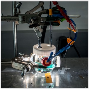
Shown is a photoelectrochemical cell illuminated by a solar simulator. A bismuth vanadate thin-film electrode is being tested in an electrolyte solution to mimic conditions in an artificial photosynthesis device. (Credit: Paul Mueller/Berkeley Lab)
One of the major challenges for scientists working to create systems that efficiently convert sunlight, water and carbon dioxide into fuel is finding materials that can do the work while also surviving the corrosive conditions that are part of the process. Existing methods to determine material stability have been hit and miss, but a Berkeley Lab-led research team has applied a combination of experimental and theoretical tools to rigorously determine how well a material will weather the harsh environments present in these systems.
“None of the existing methods to predict material stability were working,” said study lead author Francesca Toma, a Berkeley Lab staff scientist in the Chemical Sciences Division. “We need to develop a set of techniques that could give us a more accurate assessment of how a material will behave in real-world applications. How can we figure out if this material is going to last 10 years? Having methods that allow us to understand how a material degrades and to predict its stability over the years is an important advance.”
Berkeley Lab scientists at DOE’s Joint Center for Artificial Photosynthesis are working to improve systems that efficiently convert sunlight, water and carbon dioxide into fuel. Shown (left to right) are David Larson, Kristin Persson, Jeff Beeman, Ian Sharp, and Francesca Toma. (Credit: Paul Mueller/Berkeley Lab)
Artificial photosynthesis has a way to go to achieve the controlled, stable process of its natural counterpart. A key step in both natural and artificial photosynthesis is the splitting of water into its constituents, hydrogen and oxygen. In natural systems, stability of the components that perform this function is not required, since they can self-heal in living cells.
But unlike plants, practical solar fuel generators demand stable materials that do not need to be continuously replenished. Another consideration is that these devices need to operate in highly corrosive conditions that exacerbate the wear and tear on sensitive components. Unfortunately, most materials do not survive in these environments, and their performance degrades accordingly, the researchers said.
The scientists focused on bismuth vanadate, a thin-film semiconductor that has emerged as a leading candidate for use as a photoanode, the positively charged part of a photoelectric cell that can absorb sunlight to split water. Going by traditional approaches to predict material characteristics, bismuth vanadate should be resistant to chemical attack. It is not.
Shown is a cross-section of pristine (left) and damaged bismuth vanadate, a thin-film semiconductor, taken by a transmission electron microscope. The bismuth vanadate is colored yellow to highlight the contrast with the layer below. The yellow layer is intact on the left, but fragmented on the right after exposure to an alkaline bath. (Credit: Matthew McDowell/Caltech)
In reality, bismuth vanadate exhibits complex chemical instabilities that originate from kinetic limitations, which are related to the inability to structurally reorganize the surface phase such that it could reach a stable configuration under the operating conditions.
The scientists used carefully selected experimental methods to analyze bismuth vanadate before and after its use, as well as directly under operational conditions. They found an accumulation of light-generated charge at the surface of the film, which led to structural destabilization and chemical attack of the metal oxide semiconductor.
“For complex metal oxides, a significant structural reorganization is required to create a thin layer on the surface that can be thermodynamically stable, and that process can be very slow,” said Toma.
Senior authors on this study are Ian Sharp, a staff scientist in the Chemical Sciences Division, and Kristin Persson, a staff scientist in Materials Science and Engineering and in the Energy Technologies Area.
“Today, bismuth vanadate is one of the best materials available for constructing photoanodes,” said Sharp. “Ultimately, though, we need to discover new semiconductors that can more efficiently absorb light and help drive the reactions that allow us to store energy from the sun in chemical bonds.”
The researchers added that one of the next steps in understanding these materials is to study the relation between the local chemical composition and performance over different length and time scales under operating conditions.
“Understanding the origin of the degradation process is crucial to designing materials that are more resistant,” said Persson. “It is our hope that this study will spark further improvements in the screening and development of new materials with enhanced stability under operating conditions.”
This work was performed at JCAP, established in 2010 by the DOE to develop a cost-effective method of turning sunlight, water and carbon dioxide into fuel. JCAP, a DOE Energy Innovation Hub supported by the department’s Office of Science, is led by the California Institute of Technology with Berkeley Lab as a major partner. Imaging work was done at the Molecular Foundry, a DOE Office of Science User Facility.
Share on:


Testimonial
"In a year when every marketing dollar mattered, I chose to keep I-Connect007 in our 2025 plan. Their commitment to high-quality, insightful content aligns with Koh Young’s values and helps readers navigate a changing industry. "
Brent Fischthal - Koh YoungSuggested Items
Curing and Verification in PCB Shadow Areas
09/17/2025 | Doug Katze, DymaxDesign engineers know a simple truth that often complicates electronics manufacturing: Light doesn’t go around corners. In densely populated PCBs, adhesives and coatings often fail to fully cure in shadowed regions created by tall ICs, connectors, relays, and tight housings.
Marcy’s Musings: Advancing the Advanced Materials Discussion
09/17/2025 | Marcy LaRont -- Column: Marcy's MusingsAs the industry’s most trusted global source of original content about the electronics supply chain, we continually ask you about your concerns, what you care about, and what you most want to learn about. Your responses are insightful and valuable. Thank you for caring enough to provide useful feedback and engage in dialogue.
September 2025 PCB007 Magazine: The Future of Advanced Materials
09/16/2025 | I-Connect007 Editorial TeamMoore’s Law is no more, and the advanced material solutions being developed to grapple with this reality are surprising, stunning, and perhaps a bit daunting. Buckle up for a dive into advanced materials and a glimpse into the next chapters of electronics manufacturing.
I-Connect007 Launches Advanced Electronics Packaging Digest
09/15/2025 | I-Connect007I-Connect007 is pleased to announce the launch of Advanced Electronics Packaging Digest (AEPD), a new monthly digital newsletter dedicated to one of the most critical and rapidly evolving areas of electronics manufacturing: advanced packaging at the interconnect level.
Panasonic Industry will Double the Production Capacity of MEGTRON Multi-layer Circuit Board Materials Over the Next Five Years
09/15/2025 | Panasonic Industry Co., Ltd.Panasonic Industry Co., Ltd., a Panasonic Group company, announced plans for a major expansion of its global production capacity for MEGTRON multi-layer circuit board materials today. The company plans to double its production over the next five years to meet growing demand in the AI server and ICT infrastructure markets.